SOLUTIONS & SERVICES
Solutions & Services
Soldering for Electronics Packaging

Assembly Solutions
S-Bond Technologies’ active fluxless soldering for electronics offers many advantages where flux may contaminate the electronics or optics in a package. S-Bond can join metals, ceramics, graphite and composites used in a range of advanced electronic packaging, optical fibers and windows as well as bond the metallic components together. Electronic packages utilize a wide range of materials designed for a variety of functions to include heat sink lids, hermetic seals and EMI shielding. Ceramics, various metals and even composite materials are being used to engineer a specific package to its requirements and to suit operating environments. S-Bond is a versatile joining material that can join from 115 – 400C, depending on the service requirements.
Active “fluxless” soldering offers many advantages since flux may contaminate the electronics or optics in a package. S-Bond can join the optical fibers and windows as well as bond the metallic components together.
S-Bond products bond to silicon dies and MEMS without the need to coat or metallize prior to joining. These materials also join well to copper-tungsten, alumina, silicon carbide, nickel, and other materials used in lids and substrates. These capabilities offer the possibility for direct die attachment to a package lid, joining of MEMS and other devices into lead frames, and direct attachment of silicon or silicon carbide devices to heat sinks and heat spreaders.
Conventional attachment techniques using filled polymers do not offer the same level of thermal conductivity as a completely metal bond, but directly bonding to silicon and packaging materials typically requires the use of a flux or thin film metallization of the joining surfaces.
SBT offers options for bonding to silicon, metal, ceramic, or ceramic composite materials without metallization or flux, which can withstand lead free solder reflow cycles for board mounting.
Contact Us to assess the suitability of S-Bond joining of your electronic or opto-electronic packages and refer to our Technical Resources Section and Blog for the latest developments and information.
Electronic Applications

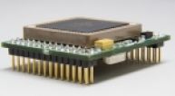
On printed circuit boards (PCBs), as shown in the image to the left, the increased use of new materials for improved thermal management and lower cost is challenging conventional joining processes. SBT products have been shown to bond to silicon dies and MEMS without the need to coat or metallize prior to joining. These materials also join well to copper-tungsten, alumina, silicon carbide, nickel, and other materials used in lids and substrates.

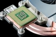
Thermal management on die packages are increasingly being used to lower their temperatures as speeds and power density increase. Direct bond of heat pipes (as shown in the figure to the left), vapor chambers and other heat spreaders will benefit from the use of metallic bonding materials as compared to other filled epoxy or polymer thermal interface materials.
Additionally, in the area of power electronics, S-Bond® materials can be used to bond IGBT modules directly to base plates of copper-tungsten, aluminum silicon carbide, aluminum nitride, and nickel coated versions of these materials.

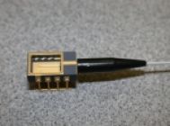
Many times fluxes may contaminate the electronics or optics in a package therefore fluxless soldering is preferred. S-Bond is well suited to join various packages as show in the figure to the left. S-Bond can join the optical fibers and windows as well as bond the metallic components together.
Contact Us with questions about soldering for electronics and let us assess the suitability of S-Bond joining of your electronic or opto-electronic packages.
More Information?
If you would like someone to contact you or provide information, please submit the information to the right.
