sbondadmin
June 10, 2019
S-Bond® Ultrasonic Active Soldering of Silica
Ronald Smith S-Bond Technologies Inc., Hatfield, PA,
Lawrence W. Shacklette, Michael R. Lange, James C. Beachboard,
Harris Corp., Melbourne, FL
and Donna L. Gerrity E&S Consulting Inc., St. Augustine, FL
Packaging of optical devices often requires the need for creating strong bonds between metal and silica. The most convenient and cost effective approach would be to directly solder to both silica and metal without requiring pre-metallization of the silica. Soldering to oxides and oxidized surfaces has been accomplished with various solders containing metals with strong affinity for oxygen, known as “active solders”.
S-Bond Technologies worked with Harris Corporation to understand S-Bond® 140 active solders, based upon a tin-bismuth eutectic with activating additives of cerium, gallium, and titanium, to produce seals between metals and silica. Titanium and cerium are energetically capable of competing for the oxygen in silica, and are therefore capable of reducing or forming mixed oxides with silica under appropriate conditions. The bond between such an “activated” solder and high purity fused silica (HPFS) has been characterized by Time-of-Flight Secondary Ion Mass Spectrometry (TOF-SIMS). Two variations of solder produced by S-Bond Technologies, S-Bond®140 and S-Bond®140 M1 were bonded to silica using a fluxless ultrasonic technique.
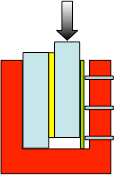
Figure 1 illustrates the ultrasonic soldering process where the resultant cavitation of the molten solder layer continually disrupts the oxides forming on the molten solder surface, enable the active elements to be in direct contact with the base materials own oxide surface, in this case silica, SiO2.

Figure 1. Illustration of ultrasonic soldering process with active solders.
To compare the influence of the active elements on the strength of the soldered bond silica to metal interfaces when using non-activated solders and active solders, a simple overlap soldered coupon ( ~ 1” x 1” ) was used on a compression lap shear test. Figure 2 illustrates the soldered specimen shear test configuration.
Figure 2. Illustration of compression lap shear test configuration.
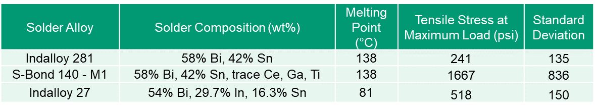
Table 1 summarizes the lap shear strengths of the active S-Bond® 140 M1 and compares its shear strength to hose of typical non-active element solders.
Table 1. Compression Lap Shear Test Results
The results in Table 1 show that the active S-Bond® 140M1 solders far exceed the shear strengths of non-active elements solders.
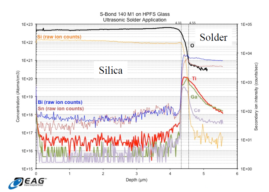
To characterize how the active elements are increasing the bond silica-metal joint strengths, Time of Flight – Secondary-ion mass spectrometry [TOF-SIMS] was used to characterize the bond interface. TOF-SIMS measured the distribution of the various S-Bond® elements as a function of depth through the interface. The results show that the activating elements (Ti, Ce, Ga) concentrate at the interface and that their oxides form the interfacial layer between the high purity silica (HPS) and the bulk solder.
The efficacy of these additives was established by demonstrating that the block shear strength of the bond to HFPS was increased by 7 times through the addition of the Ti, Ce and Ga reactive metals to the base Sn-Bi solder.
The resultant data from the investigation showed a significant increase in the concentration of all of the “active” elements present in S-Bond® 140 M1 within a 220 nm interfacial zone between the solder and HPFS.
Figure 3. Charts of Element concentrations made from S-Bond® 140M1 joints between Silica and metal using Time of Flight – Secondary-ion mass spectrometry [TOF-SIMS].
In addition to this accumulation of “active” elements, the quantitative concentration of O was higher in the interfacial region than in areas away from the interface in the solder bulk. These data support the formation of mixed oxides at the interface play a significant role in adhesion. The data also support the notion that the interface comprises an oxide to oxide bond, that is, a silica to active metal oxide bond. All three active elements present in the solder seem to participate relatively equally in this bond formation.
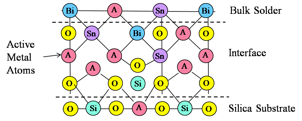
Figure 4. Illustration of mixed oxide bond interface at S-Bond® 140M1 solder to silica surface.
It cannot be necessarily concluded that each active element (Ti, Ce or Ga) has the same contribution to bond strength, or whether having an intermetallic mixed oxide offers an advantage over a simple oxide of a rare earth or titanium. Based on concentration alone, it appears that the role played by all three metals is essentially the same. The thickness of the oxide layer (220 nm) and the observation of an interface layer with mixed oxides supports the model depicted in Figure 4.
The active elements accumulate at the interface because this is the available reaction site due to the presence of the substrate oxide (silica) and potential free oxygen. Once the oxidation reaction occurs, the active metal becomes bound at the interface, and thus accumulates there. The mechanism for movement of the “active” elements to the interfacial region against an apparent concentration gradient is presumably due to mechanical forces, but could also be aided by thermal convection. The ultrasonic energy applied to the system is believed to play a key role in the observed movement of “active” elements to the interfacial region and possibly to an enhanced O level in this same region. Ultrasonic or any other form of mechanical agitation can establish a mixing of the solder that would bring active metal to the interface.
REFERENCES
[1] Nagono, K., Nomaki, K., and Saoyama, Y., US Pat. 3,949,118.
[2] Ramirez, A.G., Mavoori, H. and Jin, S., “Bonding nature of rare-earth-containing lead-free solders”, Appl. Phys. Lett. 80, 3 21, 398-400: and US Pat. 6,306,516.
[3] Tomáš Skála, Nataliya Tsud, Kevin C. Prince and Vladimír Matolín, “Bimetallic bonding and mixed oxide formation in the Ga–Pd–CeO2 system”, J. Appl. Phys. 110, 043726 (2011).
[4] A.R. Lobato, S. Lanfredi, J.F. Carvalho, A.C. Hernandes, “Synthesis, Crystal Growth and Characterization of g-Phase Bismuth Titanium Oxide with Gallium”, Mat. Res. vol.3 n.3 São Carlos July 2000.
This investigation has shown how effective active element solders, such as S-Bond 140M1 are in bonding metals to silica (SiO2) surfaces. If you have applications requiring the bonding and sealing of fused silica or related glasses, please Contact Us… and we can assist in meeting your need.

 In sputter targets, the deposition/target materials is sputtered (high energy ion impacts displace a target’s atoms) onto an opposite surface to form a functional coating or other element layer in a computer chip, TV screen or other semiconductor device. The high energy impact of the deposited films require “sputter targets” to be cooled to keep the target material layer from melting. To cool the target, water is circulated in an aluminum or copper base plate. S-Bond active solders can bond all metals and most ceramics that are commercially used to produce sputtered films. Active solders can bond these sputter targets to either Copper or Aluminum, bonding them at low temperatures (which minimizes thermal expansion mismatch stresses), without flux contamination/entrapment (which will contaminate the sputtering plasma), and with excellent thermal conductivity (a metallic bond with nearly no voids).
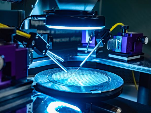 For probes and sensors, S-Bond active solders can bond silicon or carbide/carbon based devices (MEMS or other semiconductor based probes) directly to metal and metallic conductor leads. The low temperature active solders, when joining semi-conductor devices, impart low residual stresses and the joints are electrically and thermally conductive… good for signal transmittance and cooling.

 Piezo ceramic (PZT) – Ultrasonic Gas Flow sensors;
  MEMS Pressure Gages; Silicon based MEMS devices us Si-dies and incorporate circuitry to use the Si as part of the measurement. In the case of pressure measurements, thin diaphragms of Si are created and strain gage circuitry is deposited using lithography to complete the sensor… the challenge then was so seal the Si-sensor die to a metallic pressure housing that is installed onto the component needing a pressure sensor. S-Bond® active solders can join
  Graphite Electrodes / Water Conductivity Sensors; S-Bond® active solders are being used to
  Sapphire – Optical Sensors; Sapphire is single crystal aluminum oxide that is very hard/scratch resistant and also transits optical signals in a specific spectrum. As sapphire is an excellent “window” material for many optical signals. For example in Gamma Ray Detection, NaCl single crystal creates photon (light) output proportional to the impinging gamma ray radiation intensity. The NaCl crystal will degrade/dissolve in contact with air, to the crystal is housed behind a sapphire window which is
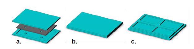
 Figure 2. Copper and Aluminum clad CarbAl-G circuit boards.
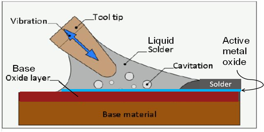

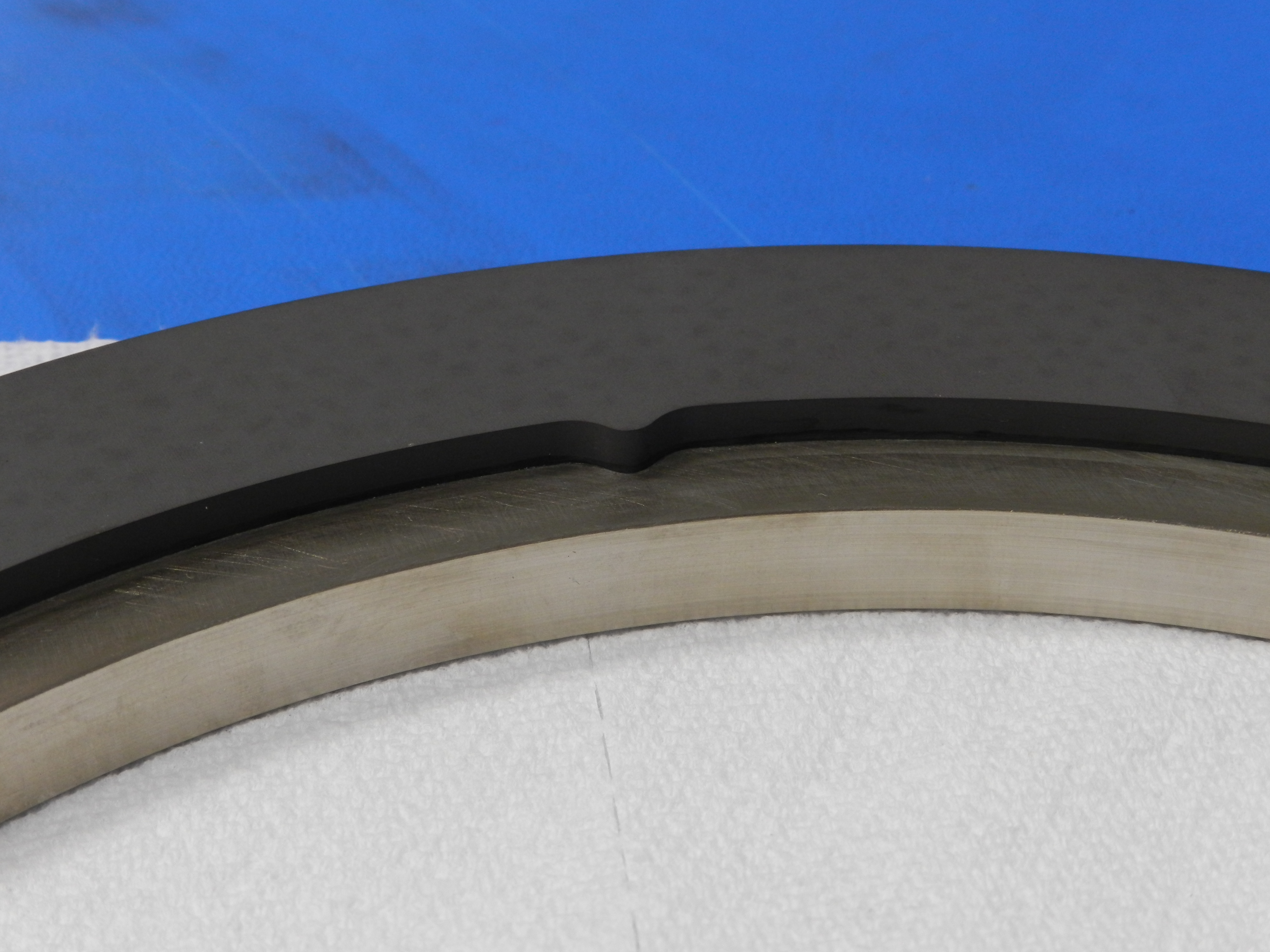
 Carbon/graphite compressor seal rings are employed in many compressors and more and more metal backed graphite seals are being used in higher efficiency compressors. Frictional heating of seals can degrade metal backed graphite seals, therefore good thermal contact between the graphite seal ring and the metal backing is needed to improve cooling of the seal.
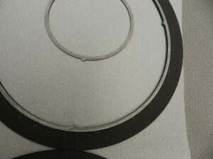
 Copper has superior cooling capacity than aluminum and is the preferred heat sink material for telecommunications and high power electronics. However, the weight and cost or copper limits the size of the heat sink packages. Therefore for larger electronic enclosures a hybrid design, using copper for a localized heat sink joined to an aluminum frame with good thermal contact can significantly improve the cooling performance of a heat sink package.
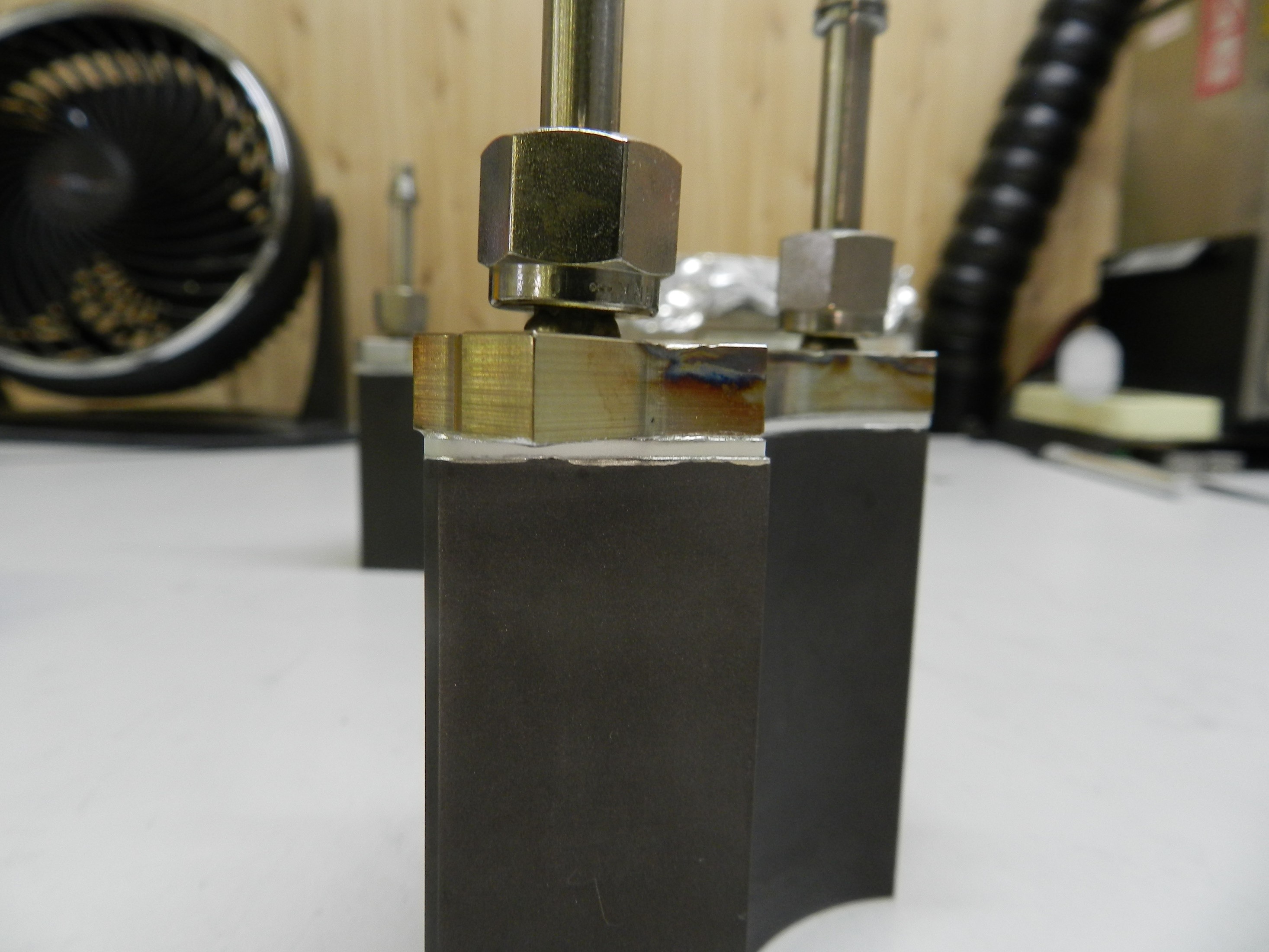
 S-Bond Technologies’ active solder joining solutions have been used by by Fermi National Accelerator Laboratory for joining carbon:carbon and pyrolytic graphite in its particle accelerator program. The improved Forward Particle Detector (FPIX) is to be used in Compact Muon Solenoid (CMS) and used for high-resolution, 3D tracking points, essential for pattern recognition and precise vertexing, all embedded in a hostile radiation environment.
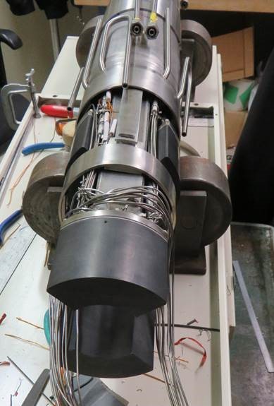
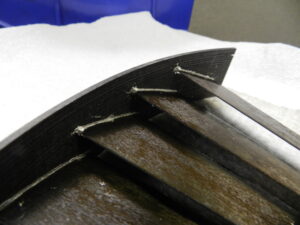
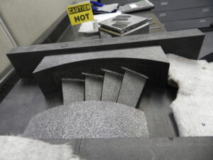
 where the blades were inserted, Figure 3. After metallization, the blade and nozzle segments were inserted into a heated alignment press, Figure 4. After heating and insertion, the nozzle segment/ TPG blade assembly was cooled and removed. Figures 1a – b, above, showed the final fully bonded assembly.