215.631.7111

S-BOND BLOG

S-Bond® Solders At the Interface of the NanoBond® Process
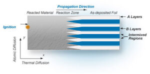
Figure 1. Illustration of the NanoBond® / NanoFoil® heating process® (from www.indiumcorp.com)

S-Bond active solder layers have been shown in many applications to be the key ingredient that permits many ceramics and refractory metals to be bonded to largely coefficient of thermal expansion (CTE) mismatched metals such as aluminum and copper. Indium Corporation offers a NanoBond® process that uses NanoFoil ® as local heat source to remelt preplaced solder layers without the need for the bulk heating of assembled components that have large CTE mismatch. Active S-Bond solders are applied as prelayers and have Ti, Ce, Ga and Mg additions that permit them to wet any ceramic or metal surface. Once the S-Bond pre-layers are applied to ceramic and/or metallic surfaces, conventional solders can be reflowed onto the S-Bond layer to create the preplaced solder layers that are remelted and bonded via the heat emitted from an ignited NanoFoil®. Figure 1 illustrates how temperatures of over 1,400 K are generated by an ignited nano-engineered foil. (more…)

Fluxless Soldering of Sputter Targets

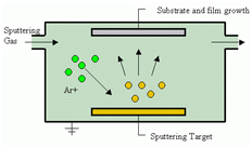
Figure 1. Schematic of sputtering process

S-Bond soldering is seeing increased application for the solder bonding of sputter targets. Sputter targets are used in a wide range of applications for making thing films used in making electronic chips, solar cells, sensors, TV screens, optical components, electrical devices, and on and on… Sputter targets support a very large physical vapor deposition (PVD) and diverse technological base that is wide ranging and pervasive. Sputter targets under ion bombardment release target material atoms into a high vacuum chamber that under an electric field can be accelerated and deposited onto the component surface where the arriving atoms arrange themselves into a contiguous thin film. Figure 1 schematically illustrates the sputtering process. Ion bombardment is a high energy collisional process that can heat target materials to their melting points unless cooled; hence most sputter targets are bonded to a water cooled backing plate. Backing plates are made normally made from copper and are mounted to a water cooling manifold. Other metallic backing materials are also used. See Figures 2-3 for examples of bonded sputter targets. (more…)

Joining Dissimilar Materials

The Issue of Coefficient of Thermal Expansion (CTE) Mismatch

Yes, S-Bond can join a wide variety of materials, including aluminum, copper, stainless steel, refractory metals and ceramic to metal brazing with aluminum oxide, aluminum nitride, silicon carbide and other oxide, nitrides and carbides… however, with this wide variety of materials joining capability, we have a lot of inquiries about aluminum soldering to stainless steel or aluminum oxide, graphite bonding to aluminum, titanium to silicon carbide, etc. (more…)