sbondadmin
April 11, 2014
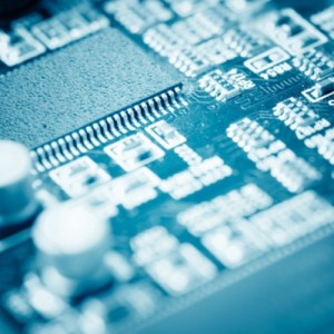
 Sapphire crystals play a key role in protecting various electronics from environmental conditions, as the material is one of the most scratch-resistant available. In fact, the latest Apple smartphone, the iPhone 5S uses it as protection both for the camera lens as well as the fingerprint scanner that is now incorporated into the front face.
It has been posited that Apple might use the crystal, synthetically produced, for the screen of the iPhone 6. The crystal is even stronger and more resistant to strikes than Corning’s Gorilla Glass, currently the standard for smartphones from a variety of manufacturers. One key concern is cost, and an Apple partner has reportedly streamlined the process. With phones and other products, another key is aluminum soldering or joining sapphire to other materials.
While many companies make electronics relatively easy to take apart to make repairs and replace components, the tech giant has a history of making closed systems. If that is the case, then joining the screen to the frame of the case could improve rigidity and limit deformation from falls or other accidents. Perhaps more importantly, any reduction in the price of sapphire display screens could spur its usage in other industries.
As noted above, phone makers already take advantage of the material to protect camera lenses, yet it is also commonly used in the production of lasers and in high-risk environments for sensor arrays, such as on oil rigs or for equipment that must take the brunt of sand, wind and other things that can degrade surfaces relatively quickly. If GT Advanced Technologies can decrease the costs of production, it stands as a material nearly as scratch-resistant as synthetic diamonds and far superior to
This will improve opportunities to make stronger electronics, but at the same time engineers will need to consider aluminum soldering options and other joining materials that can be used in low-temperature processes. Otherwise, they will be limited in designs based on differences in coefficients of thermal expansion between materials.
The report is available on the possibility of sapphire crystal production used in the upcoming iPhone 6.
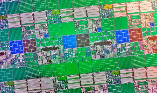 Chip-on-wafer technology could pave the way for higher-performance, slimmer and more cost-effective electronic devices.
 A way to use weak molecular bonding interactions to create well-ordered and stable metal–organic monolayers with optoelectronic properties has been found by researchers from the RIKEN Surface and Interface Science Laboratory. The development could form the basis for the scalable fabrication of molecular optoelectronic devices.