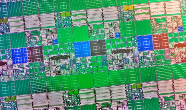
IME Forms Chip-On-Wafer Consortium
 Chip-on-wafer technology could pave the way for higher-performance, slimmer and more cost-effective electronic devices.
Conventional Chip-on-Wafer bonding techniques used for making 3D chipsets rely on a solder-assisted thermo-compression bonding process that takes more than 15 seconds at a minimum of 300 degrees Celsius to complete. This method, which attaches the chip to a piece of semiconductor wafer, slows the overall production process and results in higher manufacturing costs.
AsianScientist (Dec. 29, 2014) – A*STAR’s Institute of Microelectronics (IME) has formed a Chip-on-Wafer (CoW) Consortium to enable semiconductor firms to develop commercially-viable capabilities for making 3D chipsets.
The consortium is working on overcoming such challenges by using low temperature copper-copper (Cu-Cu) diffusion bonding.
Read more at: http://www.asianscientist.com/