ULA has recognized S-Bond Technologies with a Small Business Excellence Award for their support of the Vulcan Centaur program. As a materials technology company that provides bonding solutions for a broad range of materials, S-Bond played an integral role in providing its active solder technology in the Vulcan Soldered Transition Ring qualification.
Launch of Atlas V Juno from Cape Canaveral AFS
S-Bond active solders were instrumental in providing a seal for the Transition ring that feeds liquid oxygen into Vulcan Centaur’s main engine. These seals have undergone rigorous cryogenic testing resulting in ULA’s use of this technology.
Contact Us for more information on how S-Bond solders can solve your bonding challenge.
S-Bond Technologies’ active solders are finding wide application in semiconductor processing equipment. Their capability to join a wide range of dissimilar materials and the fact that as a filler metal, their bonds are thermally conductive make S-Bond solders far superior to many other commercial bonding/thermal interface materials. Semiconductor processing applications include…
In sputter targets, the deposition/target materials is sputtered (high energy ion impacts displace a target’s atoms) onto an opposite surface to form a functional coating or other element layer in a computer chip, TV screen or other semiconductor device. The high energy impact of the deposited films require “sputter targets” to be cooled to keep the target material layer from melting. To cool the target, water is circulated in an aluminum or copper base plate. S-Bond active solders can bond all metals and most ceramics that are commercially used to produce sputtered films. Active solders can bond these sputter targets to either Copper or Aluminum, bonding them at low temperatures (which minimizes thermal expansion mismatch stresses), without flux contamination/entrapment (which will contaminate the sputtering plasma), and with excellent thermal conductivity (a metallic bond with nearly no voids).
For probes and sensors, S-Bond active solders can bond silicon or carbide/carbon based devices (MEMS or other semiconductor based probes) directly to metal and metallic conductor leads. The low temperature active solders, when joining semi-conductor devices, impart low residual stresses and the joints are electrically and thermally conductive… good for signal transmittance and cooling.
Piezoceramics such as Pb-Zirconates (PZT) that impart force/small displacement or create ultrasonic pulses, can be bonded direct to metals with active solders. Bonding is accomplished bonded below their curie points with acoustically sound interfaces that can transmit sound effectively. Such piezoceramic based sensors and actuators are used in accurately measuring gas flow and can be used on gas control in MOCVD processes used to deposit and etch computer chips. S-Bond active solders can wet and adhere to most piezoceramics all without pre-plating and chemical fluxes… as such they are finding excellent application in probes and sensors used on semiconductor processing.
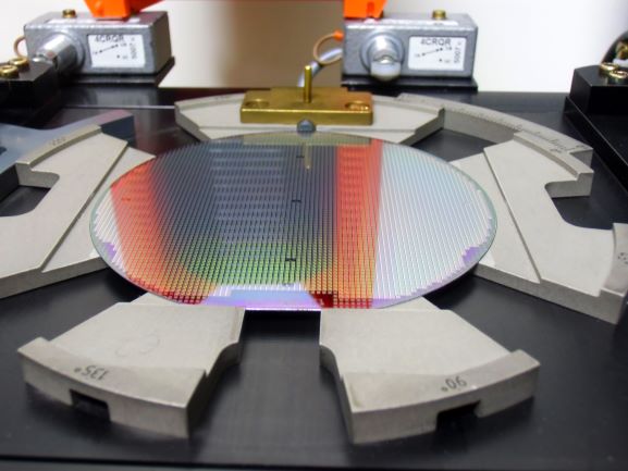
Wafers (silicon or other) are placed into energetic plasmas and other beams to deposit then etch a complicated surface morphology in layers to create semiconductor based chips. The high heat energy into the wafer needs to be removed through water cooled wafer handling devices such as the pedestals the wafer sits on in their processing chambers. If not cooled, the interdiffusion of the fabricated on the wafer. With the latest 300mm diameter wafer technology over a $1M work of chips can be on a wafer.
The high energy levels used in semiconductor processing requires well cooled and reliable handling equipment. S-Bond active solders can intimately join copper and aluminum as well as other thermal management materials such as AlSiC and pyrolytic graphite.
If you would like to see how S-Bond active solders can improve your semiconductor processes and handling and measuring equipment, please Contact US.
Sensors and actuators are a growing commercial market with the Internet of Things (IOT) and the interest to remotely monitor and control many devices.
S-Bond® active solders are finding more application in sensors and actuator devices due to their use of dissimilar materials, including metals, intermetallics, ceramics, composites and glasses which need to be joined. S-Bond® active solders are unique in that they can join such materials, without flux or plating, at low temperatures and with excellent conductivity (both electrical and thermal).
With Ce, Ga and Ti additions to solder filler metals, S-Bond® solders can bond direct to oxides, nitrides and carbides that have formed on metal surfaces, directly. On aluminum and copper the Ga and Ce interact with the oxides that form on these metals then the Sn and Ag constituents form metallurgical intermetallic compounds (IMC’s) that chemically bind the solder to the aluminum or copper base metal. With the active S-Bond® solders’ ability to wet, adhere and join such a diverse set of materials, the S-Bond® alloys find wide application in sensors and actuators that employ a diverse array of materials and in dissimilar material joints… These joints have many requirements, depending on the application, these requirements include…
Thermally conductive
Electrically conductive
Transmits sound
Hermetically seals
Bond strengths high enough for the application
Low temperature joining
Accommodation of CTE mismatch strain
Sensors and Actuators that S-Bond® is currently specified in includes…
Piezo ceramic (PZT) – Ultrasonic Gas Flow sensors; PZT ceramic disks are S-Bond® soldered to stainless steel housings that transmit and receive u/s sound pressure waves. The transmit sensor with bonded PZT piezo ceramic disk sends u/s waves into a passing gas flow and a receive sensor with bonded PZT receives and converts the sound waves… with a shift in frequency known as the Doppler effect, can relate the frequency shift to the mass flow of the passing gas stream. In these sensors, the piezo ceramic disk needs to be intimately bonded with no voids to create an acoustically “hard” transmitting bond interface, joining the ceramic to metal below the curie temperatures of 250 C. S-Bond® 220 alloys are being used to make these reliable and acoustically sound interfaces.
MEMS Pressure Gages; Silicon based MEMS devices us Si-dies and incorporate circuitry to use the Si as part of the measurement. In the case of pressure measurements, thin diaphragms of Si are created and strain gage circuitry is deposited using lithography to complete the sensor… the challenge then was so seal the Si-sensor die to a metallic pressure housing that is installed onto the component needing a pressure sensor. S-Bond® active solders can join Si direct to metals and can create a hermetic joint, creating a seal between the Si-MEMS pressure sensor and the mounting housing.
Graphite Electrodes / Water Conductivity Sensors; S-Bond® active solders are being used to join graphite to electrical leads for use in Anode/Cathode systems for making excellent electrical solder connections with the use of flux or pre-plating.
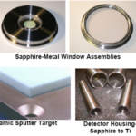
Sapphire – Optical Sensors; Sapphire is single crystal aluminum oxide that is very hard/scratch resistant and also transits optical signals in a specific spectrum. As sapphire is an excellent “window” material for many optical signals. For example in Gamma Ray Detection, NaCl single crystal creates photon (light) output proportional to the impinging gamma ray radiation intensity. The NaCl crystal will degrade/dissolve in contact with air, to the crystal is housed behind a sapphire window which is S-Bond® active solder sealed (hermetic/He leak free) to a titanium tube to create a sealed environment that the gamma rays can penetrate. Optical detectors are then mounted in front of the sapphire window, outside the S-Bond® sealed enclosure.
Insulators /Radar Sensors; Printed 3-D circuits are being made to generate / receive radar signals. These circuits are built through ceramic layers that form a ceramic backbone to the sensors’ circuitry. S-Bond® active solders have been used to bond the edges of this ceramic backbone of the sensor and seals it from the environment.
Magnet Assemby – Actuators; Magnetic actuators are used to move valves, switches and other devices dependent on precise and reliable stroke based motion. Such magnetic actuators are using high force as CoSm based magnets. These magnets will form a strong and specific magnet fields. In one actuator design, the actuator “rod” runs on the magnet assemblies’ magnetic axis. To assure optimal actuator lineal translation, the actuator’s central push rod could not be magnetic, so it a ceramic rod was selected. In this actuator, S-Bond® active solders have been used to bond the central ceramic rod to the magnetic core of the actuator.
As presented here, S-Bond® solders are being applied in a growing range of sensors and actuators. If you would like to take advantage of S-Bond® solders unique capabilities to join dissimilar materials in your sensors and actuators, please Contact Us.
Ronald Smith S-Bond Technologies Inc., Hatfield, PA,
Lawrence W. Shacklette, Michael R. Lange, James C. Beachboard, Harris Corp., Melbourne, FL
and Donna L. Gerrity E&S Consulting Inc., St. Augustine, FL
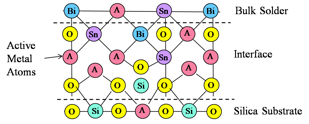
Packaging of optical devices often requires the need for creating strong bonds between metal and silica. The most convenient and cost effective approach would be to directly solder to both silica and metal without requiring pre-metallization of the silica. Soldering to oxides and oxidized surfaces has been accomplished with various solders containing metals with strong affinity for oxygen, known as “active solders”.
S-Bond Technologies worked with Harris Corporation to understand S-Bond® 140 active solders, based upon a tin-bismuth eutectic with activating additives of cerium, gallium, and titanium, to produce seals between metals and silica. Titanium and cerium are energetically capable of competing for the oxygen in silica, and are therefore capable of reducing or forming mixed oxides with silica under appropriate conditions. The bond between such an “activated” solder and high purity fused silica (HPFS) has been characterized by Time-of-Flight Secondary Ion Mass Spectrometry (TOF-SIMS). Two variations of solder produced by S-Bond Technologies, S-Bond®140 and S-Bond®140 M1 were bonded to silica using a fluxless ultrasonic technique.
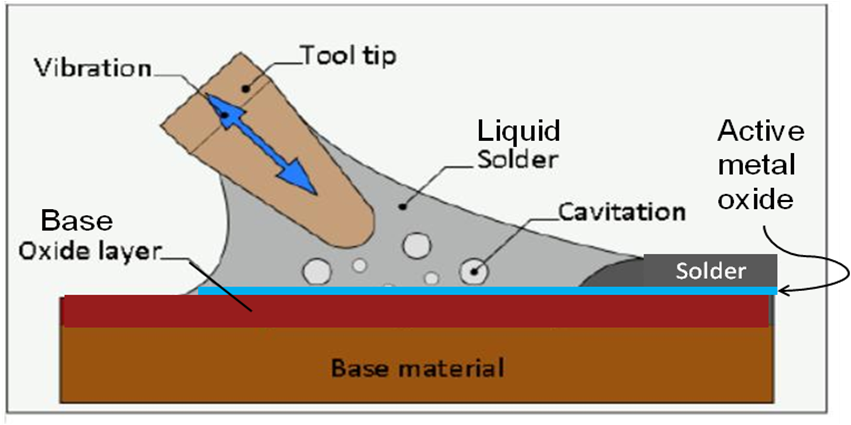
Figure 1 illustrates the ultrasonic soldering process where the resultant cavitation of the molten solder layer continually disrupts the oxides forming on the molten solder surface, enable the active elements to be in direct contact with the base materials own oxide surface, in this case silica, SiO2.
Figure 1. Illustration of ultrasonic soldering process with active solders.
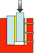
To compare the influence of the active elements on the strength of the soldered bond silica to metal interfaces when using non-activated solders and active solders, a simple overlap soldered coupon ( ~ 1” x 1” ) was used on a compression lap shear test. Figure 2 illustrates the soldered specimen shear test configuration.
Figure 2. Illustration of compression lap shear test configuration.
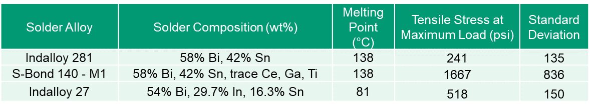
Table 1 summarizes the lap shear strengths of the active S-Bond® 140 M1 and compares its shear strength to hose of typical non-active element solders.
Table 1. Compression Lap Shear Test Results
The results in Table 1 show that the active S-Bond® 140M1 solders far exceed the shear strengths of non-active elements solders.
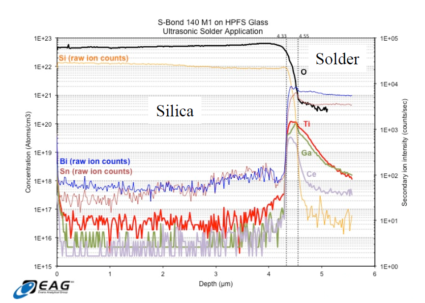
To characterize how the active elements are increasing the bond silica-metal joint strengths, Time of Flight – Secondary-ion mass spectrometry [TOF-SIMS] was used to characterize the bond interface. TOF-SIMS measured the distribution of the various S-Bond® elements as a function of depth through the interface. The results show that the activating elements (Ti, Ce, Ga) concentrate at the interface and that their oxides form the interfacial layer between the high purity silica (HPS) and the bulk solder.
The efficacy of these additives was established by demonstrating that the block shear strength of the bond to HFPS was increased by 7 times through the addition of the Ti, Ce and Ga reactive metals to the base Sn-Bi solder.
The resultant data from the investigation showed a significant increase in the concentration of all of the “active” elements present in S-Bond® 140 M1 within a 220 nm interfacial zone between the solder and HPFS.
Figure 3. Charts of Element concentrations made from S-Bond® 140M1 joints between Silica and metal using Time of Flight – Secondary-ion mass spectrometry [TOF-SIMS].
In addition to this accumulation of “active” elements, the quantitative concentration of O was higher in the interfacial region than in areas away from the interface in the solder bulk. These data support the formation of mixed oxides at the interface play a significant role in adhesion. The data also support the notion that the interface comprises an oxide to oxide bond, that is, a silica to active metal oxide bond. All three active elements present in the solder seem to participate relatively equally in this bond formation.
Figure 4. Illustration of mixed oxide bond interface at S-Bond® 140M1 solder to silica surface.
It cannot be necessarily concluded that each active element (Ti, Ce or Ga) has the same contribution to bond strength, or whether having an intermetallic mixed oxide offers an advantage over a simple oxide of a rare earth or titanium. Based on concentration alone, it appears that the role played by all three metals is essentially the same. The thickness of the oxide layer (220 nm) and the observation of an interface layer with mixed oxides supports the model depicted in Figure 4.
The active elements accumulate at the interface because this is the available reaction site due to the presence of the substrate oxide (silica) and potential free oxygen. Once the oxidation reaction occurs, the active metal becomes bound at the interface, and thus accumulates there. The mechanism for movement of the “active” elements to the interfacial region against an apparent concentration gradient is presumably due to mechanical forces, but could also be aided by thermal convection. The ultrasonic energy applied to the system is believed to play a key role in the observed movement of “active” elements to the interfacial region and possibly to an enhanced O level in this same region. Ultrasonic or any other form of mechanical agitation can establish a mixing of the solder that would bring active metal to the interface.
REFERENCES
[1] Nagono, K., Nomaki, K., and Saoyama, Y., US Pat. 3,949,118.
[2] Ramirez, A.G., Mavoori, H. and Jin, S., “Bonding nature of rare-earth-containing lead-free solders”, Appl. Phys. Lett. 80, 3 21, 398-400: and US Pat. 6,306,516.
[3] Tomáš Skála, Nataliya Tsud, Kevin C. Prince and Vladimír Matolín, “Bimetallic bonding and mixed oxide formation in the Ga–Pd–CeO2 system”, J. Appl. Phys. 110, 043726 (2011).
[4] A.R. Lobato, S. Lanfredi, J.F. Carvalho, A.C. Hernandes, “Synthesis, Crystal Growth and Characterization of g-Phase Bismuth Titanium Oxide with Gallium”, Mat. Res. vol.3 n.3 São Carlos July 2000.
This investigation has shown how effective active element solders, such as S-Bond 140M1 are in bonding metals to silica (SiO2) surfaces. If you have applications requiring the bonding and sealing of fused silica or related glasses, please Contact Us… and we can assist in meeting your need.
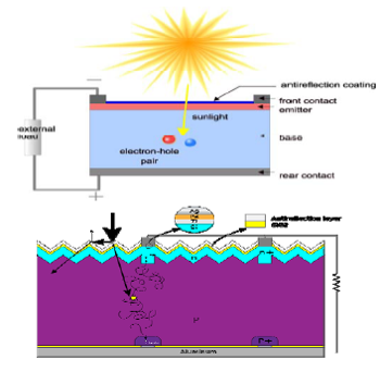
In recent years, active solders have made their way into use in solar panel manufacture. To understand where S-Bond solder alloys are being used one has to understand the solar panel construction. Solar panels consist of arrays of solar cells, soldered together. A solar cell consists of three basic elements, top contact, base and rear contact, as shown in Figure 1. From the back of each solar cell, electrical contact needs to be made between these surfaces to close the circuit and provide an electron path as photons emit electrons in the semiconductor polysilicon photovolatic (PV) cell which migrate to the back of the exposed cell surface, as illustrated.
Carrying water to the space station is a real challenge and cost, hence recycling water is critical. Waste water, sweat and other ISS water is constantly recycled in a complex system that evaporates and condenses clean water for reuse. For more information on the space station recycling system see the following link: Water Recovery System.
Thermal interface materials are materials used in creating heat conductive paths at interfaces between components and thus reduce thermal interface resistance. These materials permit more effective heat flow between separate components where heat is being generated to a heat dissipation components such as solid state transistors to heat sink or a high frequency device connected to a heat spreader. Thermal interface materials’ purpose is to fill the air gap that occurs at contact interfaces with more thermally conductive compounds to permit more effective heat flow than poorly conductive air.
There is a wide variety of thermal interface materials (TIM’s); thermal greases, phase change polymers, thermal tapes, gap filling pads, filled epoxies and solders. All having various costs, performance and manufacturing challenges.
Figure 1. Illustration of thermal grease filling an interface between a heat generating device and a heat sink.
Thermal greases are viscous fluid substance which increase the thermal conductivity of a thermal interface “gap by filling microscopic air-gaps present due to the imperfectly flat and smooth surfaces of the components as seen in Figure 1.
Thermal grease compounds have far greater thermal conductivity than air (but far less than metals). They are used in electronics, as depicted in Figure 2, to improve the heat flow from lower power electronic devices thus lowering the components temperature and increasing its life.
Bond assembly can be done via 1) mechanical attachment, 2) adhesive bonding of which epoxy bonding is one form of adhesive, 3) soldering bonding using lower melting filler metals (< 450˚C), 4) brazing using filler metals melting above 450˚C and 5) welding such as resistance welding bonding, ultrasonic welding and friction weld bonding that uses locally melted parent metal.
Bonding is done for a variety of technical reasons a) mechanical attachment, b) thermal contact, c) electrical contact d) gas or liquid seal, or e) any of all combinations of a – d. The choice of bonding method will then depend on the intrinsic properties of the bonding filler materials (hermetic, electrical conductance, thermal conductance, thermal coefficient of expansion, adhesive bond strength related to the intrinsic fillers’ mechanical properties and their adhesive and cohesive strengths…
With all these variables and design considerations how does one choose? The three main guiding principles are:
1. Cost of filler and Cost of bonding processes
2. Performance in Service (based on the properties of the bond and bonding materials)
3. Compatibility with Manufacturing Sequence.
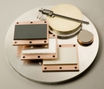
To compare epoxy bonds to solder bonds one has to ask the purpose of the bond… Is strictly a mechanical bond ? Is cost a large factor? If cost drives the choice then many times epoxy is the bonding material of choice. Epoxies are generally low cost thermosetting polymers, that are mixed chemicals which are thermally or UV cured to achieve hardness and adherence. Epoxy by far is the lower cost material over solder metal fillers and thus if low cost is the driving aim of the bond, then epoxy will be the bonding material selected. Figures 1-2 illustrate typical epoxy bonded applications
Figure 1. Epoxy bond on heat sink (courtesy of MasterBond®)
Figure 2. Epoxy seal on tube (courtesy of MasterBond®)
When bonds have to be thermally conductive or electrically conductive solders are usually the bonding material of choice. Solder are metal fillers melt below 450˚C are normally alloys of Sn, Ag, Pb, In, or Bi with the Pb-free alloys being preferred for environmental reasons. As metals, these materials are intrinsically 10 – 100 time more conductive than epoxy bonds. In recent year epoxy bonds have been filled with aluminum or silver particles to increase the epoxy bond filler conductivity to values of 3 – 5 W/m-K from 0.5 – 2 W/m-K. When compared to solder bond metals with conductivities of 40 – 400 W-m-K, one can see for thermal bonded components that solder bonding would be preferred. S-Bond Technologies makes active solder alloys that bond to metals, ceramics, glass and their combinations without the need for flux or plating and are many times selected over epoxy bonds for their improved thermal characteristics. Figures 3 – 4 illustrate typical solder bond applications.
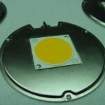
Figure 3. Solder bond LED package to heat spreader. (S-Bond® Technologies)
Figure 4. Solder bond seal of windows in housings. (S-Bond® Technologies)
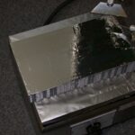
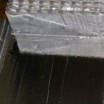
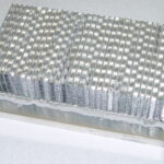
Figures 5-7 show the solder bond process being used to make a heat exchanger.
Figure 5.
Figure 6. Solder bond assembly of heat exchanger. (S-Bond® Technologies)
Figure 7. Final solder bond of finned aluminum heat exchanger. (S-Bond® Technologies)
Bonding for electrical resistance or conductance will many times determine the choice of epoxy bonds over solder or active solders. If the bond joint has to provide electrical isolation, then epoxy has much higher dielectric strength and resistivity, hence are excellent at isolating electrical components from their base materials. However, if the bond has to be electrically conductive solder bonds are preferred.
Bonding for seals are a mixed choice… in the short term epoxy seals can perform and create a sufficient seal for liquids and many gases. However, in applications for long term use epoxy bonds are permeable to certain gases and moisture and are not used in seals that require high hermetic seal integrity. Metals are impervious to moisture and gases thus solder bonds are the preferred bonding materials for high integrity hermetic seals.
Epoxy bonds are “permanent” and less resistant to thermal cycle and temperatures as well as UV exposures (can degrade with time). Solders on the other hand being metallic can be remelted repeatedly to renew or rework the bond. Additionally, as metals, solders are resistant to cracking being ductile and tough and are not susceptible to UV degradation.
Finally, the issue of compatibility with manufacturing sequences and the choice of solder bond vs. epoxy one has to select the bonding materials that will suit not only cost but the sequence of manufacturing operations. The bond has to have the properties that will take the exposure to all the assemblies operations. Bonding is many times completed after machining and fabrication but before plating or coating. If an electrical package the bonding has to be done in a compatible sequence with the electrical soldering operations. For example if a printed circuit board needs to bonded to a heat sink solder bonding the circuit board has to be done a temperatures below the solder reflow temperature on the circuit, for example below 200˚C or one has to epoxy bond the circuit board with a thermally filled epoxy. Compared to solder bonding, epoxy bonds can be less expensive in a manufacturing operation with no need for heating and reflowing solders. On the other hands solders “cure” as soon as the heating is off, while epoxy bonds need “setting time” to cure, which in some high volume applications provide some problems. When electroplating a full assembly, the bonded parts need to be bonded electrically hence solder bonding is the choice, while if powder coating, the epoxy bond may be the bond of choice.
This blog discussed how the choice of epoxy bond vs. solder bond is determined by a host of factors that need to be considered. We hope the discussion has been useful.
If you need help in making the choice of epoxy bond vs. solder please contact us, we can offer the proper counsel for making the right choice and we also offer alternative
S-Bond Technologies has developed and proven a new, lower temperature active solder that melts from 135 – 140°C. The solder, S-Bond® 140 is based around the Bismuth-Tin (Bi-Sn) eutectic composition. This new solder is a lower temperature active solder that enables multi-step soldering where previously soldered connections/seals are not remelted. Active solders that melt below 150C are also finding use in thermally sensitive applications where Sn-Ag based solders that melt over 215°C can thermally degrade the component parts being assembled. Lower temperature soldering also can more effectively bond dissimilar materials where thermal expansion mismatch many times fractures or distorts an assembly’s component parts.
S-Bond 140 is already finding application in glass-metal seals in electronic packages where higher temperature soldering alloys would have damaged the packages’ components. S-Bond 140 is also being used to bond heat pipes and vapor chamber thermal management devices to protect the thermally sensitive phase change fluids from damaging the devices when solder bonding to electronic and LED devices.
Electro-optical package to be bonded to heat sink with S-Bond® 140
S-Bond soldering is seeing increased application for the solder bonding of sputter targets. Sputter targets are used in a wide range of applications for making thing films used in making electronic chips, solar cells, sensors, TV screens, optical components, electrical devices, and on and on… Sputter targets support a very large physical vapor deposition (PVD) and diverse technological base that is wide ranging and pervasive. Sputter targets under ion bombardment release target material atoms into a high vacuum chamber that under an electric field can be accelerated and deposited onto the component surface where the arriving atoms arrange themselves into a contiguous thin film. Figure 1 schematically illustrates the sputtering process. Ion bombardment is a high energy collisional process that can heat target materials to their melting points unless cooled; hence most sputter targets are bonded to a water cooled backing plate. Backing plates are made normally made from copper and are mounted to a water cooling manifold. Other metallic backing materials are also used. See Figures 2-3 for examples of bonded sputter targets. (more…)

 In sputter targets, the deposition/target materials is sputtered (high energy ion impacts displace a target’s atoms) onto an opposite surface to form a functional coating or other element layer in a computer chip, TV screen or other semiconductor device. The high energy impact of the deposited films require “sputter targets” to be cooled to keep the target material layer from melting. To cool the target, water is circulated in an aluminum or copper base plate. S-Bond active solders can bond all metals and most ceramics that are commercially used to produce sputtered films. Active solders can bond these sputter targets to either Copper or Aluminum, bonding them at low temperatures (which minimizes thermal expansion mismatch stresses), without flux contamination/entrapment (which will contaminate the sputtering plasma), and with excellent thermal conductivity (a metallic bond with nearly no voids).
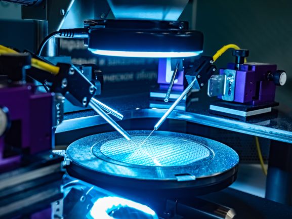 For probes and sensors, S-Bond active solders can bond silicon or carbide/carbon based devices (MEMS or other semiconductor based probes) directly to metal and metallic conductor leads. The low temperature active solders, when joining semi-conductor devices, impart low residual stresses and the joints are electrically and thermally conductive… good for signal transmittance and cooling.

 Piezo ceramic (PZT) – Ultrasonic Gas Flow sensors;
  MEMS Pressure Gages; Silicon based MEMS devices us Si-dies and incorporate circuitry to use the Si as part of the measurement. In the case of pressure measurements, thin diaphragms of Si are created and strain gage circuitry is deposited using lithography to complete the sensor… the challenge then was so seal the Si-sensor die to a metallic pressure housing that is installed onto the component needing a pressure sensor. S-Bond® active solders can join
  Graphite Electrodes / Water Conductivity Sensors; S-Bond® active solders are being used to
 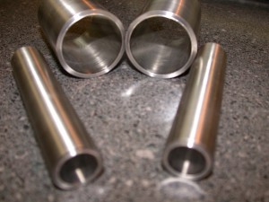 Sapphire – Optical Sensors; Sapphire is single crystal aluminum oxide that is very hard/scratch resistant and also transits optical signals in a specific spectrum. As sapphire is an excellent “window” material for many optical signals. For example in Gamma Ray Detection, NaCl single crystal creates photon (light) output proportional to the impinging gamma ray radiation intensity. The NaCl crystal will degrade/dissolve in contact with air, to the crystal is housed behind a sapphire window which is