215.631.7111

S-BOND BLOG

Bonding Graphite –Ceramic – Stainless Steel Composite Component For Los Alamos National Laboratories

Fabricating Parts for Proton Collimator With S-Bond® Active Solders®
The unique capability of S-Bond solders to join graphite and ceramic to metals was the solution for Los Alamos for fabricating core elements of their Proton Collimator used in its Proton Radiography facility. Conventional brazing was considered but their large differences in Coefficient of Thermal Expansions (CTE’s) limited brazing since on cooling from brazing temperatures (over 800°C), the resultant CTE derived residual stresses would have likely cracked the ceramic, graphite or torn the bond interface. Figure 1 illustrates the graphite – ceramic-stainless steel composite assembly that required stable, thermally and electrical conductive connection between the assembly’s elements.

Los Alamos researchers reached out to S-Bond Technologies to use its S-Bond solders to join these disparate materials. Normally plating would have to be used to make the ceramic and graphite materials solderable. In the case of S-Bond joining, the same solder and soldering process was used to make the joint between the graphite base, the insulating alumina sheet and the stainless steel plate, as depicted in Figure 1.

Figure1AProtonColimator

Figure 1. Illustration of the proton collimator elements joined with S-Bond solders.

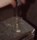
The soldering of this composite started the S-Bond metallization of the bonding surfaces of the graphite base and the alumina insulator. In this process, S-Bond metallization paste was applied to the one surface of the graphite and the two opposite sides of the alumina paste. The graphite and the alumina sheet with pastes applied, were heated to 960C in a vacuum furnace in order to react the elements in the paste with the graphite and ceramic surfaces to create a chemical bond between the solder and the graphite and alumina.  After metallization these parts’ surfaces are solderable with a well bonded interface. The Graphite base, the alumina insulator plate and the stainless steel header were heated to 250C where S-Bond 220 solder filler metal was applied via melting on and mechanical activation (spreading by heated blade or bush) to pre-tin the faying surfaces of the assembly. Once the S-Bond solder filler metal was pre-placed (pre-tinned) the parts kept hot at 250C, were placed together in an alignment fixture to align the constituent parts accurately and then pressed / loaded with 50 lbs of deadweight as the bonded assembly was cooled.

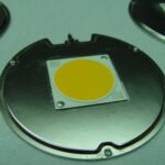
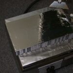
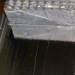
Figures 2 illustrates the solder bonded composite proton beam collimator component. The pictures show the two S-Bond solder interfaces connecting the water cooled Stainless steel end plate, to the ceramic insulator plate, then connected to the graphite cathode.

Figure2aProtonColimator
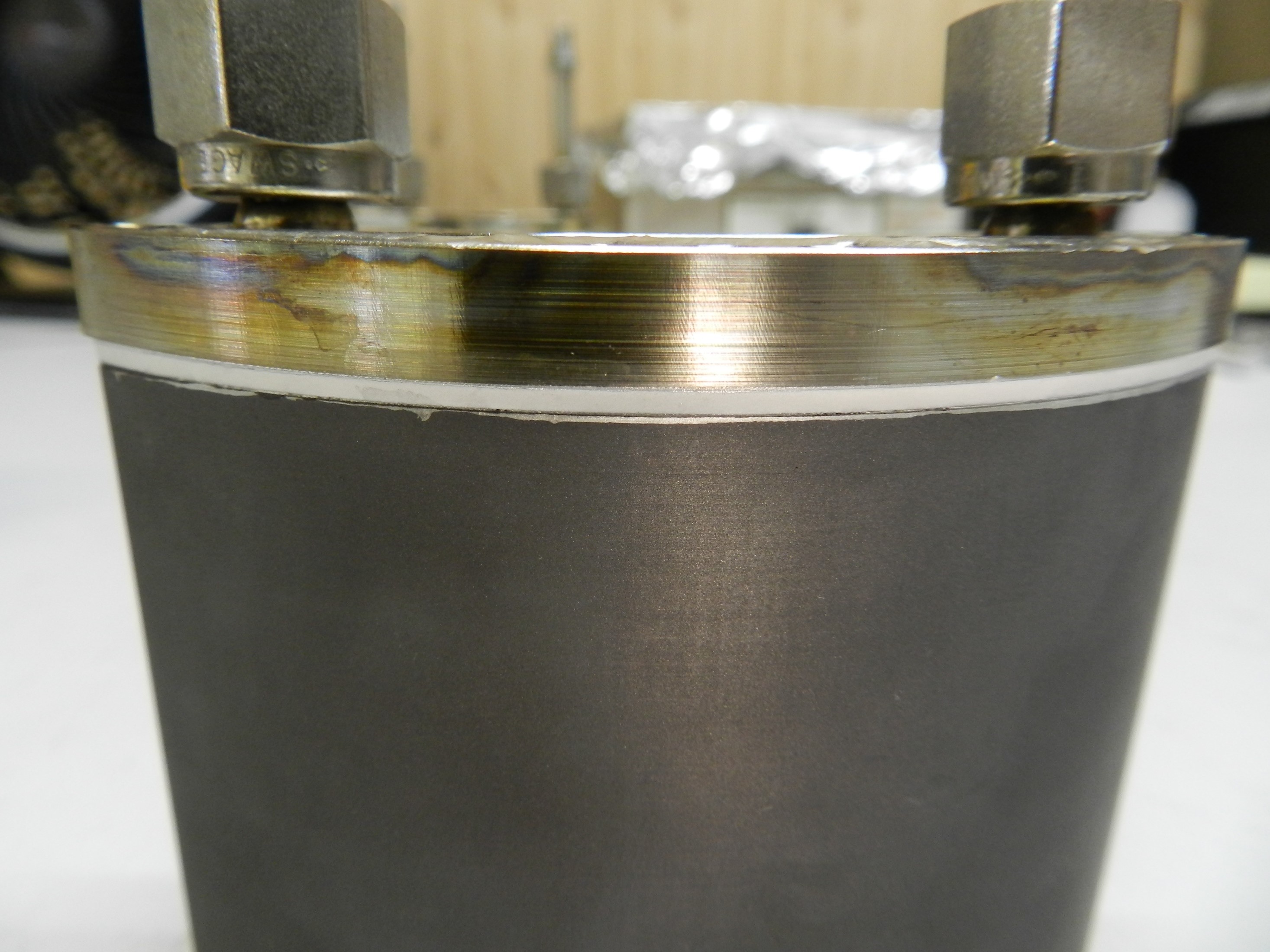
Figure 2a. Back of S-Bond joined collimator part. Stainless Steel/ceramic insulator/graphite base (from Top to Bottom)

Figure2bProtonColimator
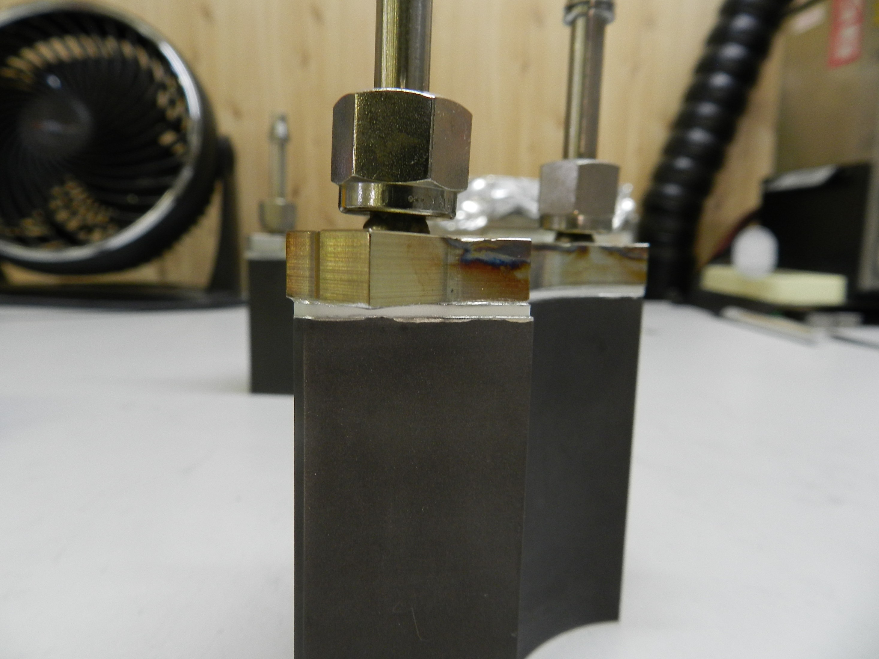
Figure 2b. Side view of S-Bond joined collimator part.

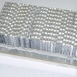
Figure 3 illustrates the Proton Collimator with the S-Bond joined parts being assembled at Los Alamos National Laboratory (LANL). There were two S-Bond joined parts per assembly. These bonded component assemblies worked very well and enables LANL engineers to successfully implement their design.

Figure3ProtonColimator

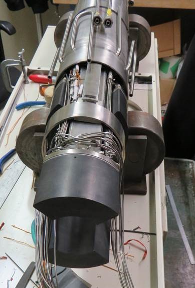
Figure 3. Proton Collimator with two S-Bond joined composite being mounted.

LANL engineers were able to utilize S-Bond’s unique capability to solder join stainless steel to ceramic to graphite. If you have such joining challenges, Contact Us for incorporating S-Bond joining in your assemblies.


Myths Regarding Lead-Free Solder Products and Joining Techniques

Soldering Techniques - Joing Methods
Brush Application

While it has been several years since manufacturers began moving to lead-free solder procedures, in part due to the European Union’s Restriction of Hazardous Substances Directive, some still believe myths that have long been inaccurate regarding the use of alloy joining materials that do not require flux and are based on lead and tin.

Temperatures Can Be Enough to Destroy Components

The first round of lead-free solder options to join metals and other materials were comprised of tin, silver and copper, which do have a slightly higher melting point of 217 degrees Celsius compared to existing solder’s 183 degrees Celsius. That disparity could cause problems regarding PC board damage.

However, newer products including several offered by S-Bond have significantly lower melting points that make it easier to join metals like aluminum. At the lowest temperatures, some materials can be joined at just 115 degrees Celsius.

Issues Regarding Silicon Will Require Other Materials

(more…)

Solder Bond vs. Epoxy Bond as Thermal Interface Materials (TIM)

Thermal interface materials are materials used in creating heat conductive paths at interfaces between components and thus reduce thermal interface resistance. These materials permit more effective heat flow between separate components where heat is being generated to a heat dissipation components such as solid state transistors to heat sink or a high frequency device connected to a heat spreader. Thermal interface materials’ purpose is to fill the air gap that occurs at contact interfaces with more thermally conductive compounds to permit more effective heat flow than poorly conductive air.

There is a wide variety of thermal interface materials (TIM’s); thermal greases, phase change polymers, thermal tapes, gap filling pads, filled epoxies and solders. All having various costs, performance and manufacturing challenges.

S-Bond Thermal Interface
Figure 1. Illustration of thermal grease filling an interface
between a heat generating device and a heat sink.

Thermal greases are viscous fluid substance which increase the thermal conductivity of a thermal interface “gap by filling microscopic air-gaps present due to the imperfectly flat and smooth surfaces of the components as seen in Figure 1.

Thermal grease compounds have far greater thermal conductivity than air (but far less than metals). They are used in electronics, as depicted in Figure 2, to improve the heat flow from lower power electronic devices thus lowering the components temperature and increasing its life.

(more…)

Epoxy Bond vs. Solder Bond Applications

Bond assembly can be done via 1) mechanical attachment, 2) adhesive bonding of which epoxy bonding is one form of adhesive, 3) soldering bonding using lower melting filler metals (< 450˚C), 4) brazing using filler metals melting above 450˚C and 5) welding such as resistance welding bonding, ultrasonic welding and friction weld bonding that uses locally melted parent metal.

Bonding is done for a variety of technical reasons a) mechanical attachment, b) thermal contact, c) electrical contact d) gas or liquid seal, or e) any of all combinations of a – d. The choice of bonding method will then depend on the intrinsic properties of the bonding filler materials (hermetic, electrical conductance, thermal conductance, thermal coefficient of expansion, adhesive bond strength related to the intrinsic fillers’ mechanical properties and their adhesive and cohesive strengths…

With all these variables and design considerations how does one choose? The three main guiding principles are:

1. Cost of filler and Cost of bonding processes

2. Performance in Service (based on the properties of the bond and bonding materials)

3. Compatibility with Manufacturing Sequence.

To compare epoxy bonds to solder bonds one has to ask the purpose of the bond… Is strictly a mechanical bond ? Is cost a large factor? If cost drives the choice then many times epoxy is the bonding material of choice. Epoxies are generally low cost thermosetting polymers, that are mixed chemicals which are thermally or UV cured to achieve hardness and adherence. Epoxy by far is the lower cost material over solder metal fillers and thus if low cost is the driving aim of the bond, then epoxy will be the bonding material selected.
Figures 1-2 illustrate typical epoxy bonded applications


When bonds have to be thermally conductive or electrically conductive solders are usually the bonding material of choice. Solder are metal fillers melt below 450˚C are normally alloys of Sn, Ag, Pb, In, or Bi with the Pb-free alloys being preferred for environmental reasons. As metals, these materials are intrinsically 10 – 100 time more conductive than epoxy bonds. In recent year epoxy bonds have been filled with aluminum or silver particles to increase the epoxy bond filler conductivity to values of 3 – 5 W/m-K from 0.5 – 2 W/m-K. When compared to solder bond metals with conductivities of 40 – 400 W-m-K, one can see for thermal bonded components that solder bonding would be preferred. S-Bond Technologies makes active solder alloys that bond to metals, ceramics, glass and their combinations without the need for flux or plating and are many times selected over epoxy bonds for their improved thermal characteristics.
Figures 3 – 4 illustrate typical solder bond applications.

Figures 5-7 show the solder bond process being used to make a heat exchanger.


Bonding for electrical resistance or conductance will many times determine the choice of epoxy bonds over solder or active solders. If the bond joint has to provide electrical isolation, then epoxy has much higher dielectric strength and resistivity, hence are excellent at isolating electrical components from their base materials. However, if the bond has to be electrically conductive solder bonds are preferred.

Bonding for seals are a mixed choice… in the short term epoxy seals can perform and create a sufficient seal for liquids and many gases. However, in applications for long term use epoxy bonds are permeable to certain gases and moisture and are not used in seals that require high hermetic seal integrity. Metals are impervious to moisture and gases thus solder bonds are the preferred bonding materials for high integrity hermetic seals.

Epoxy bonds are “permanent” and less resistant to thermal cycle and temperatures as well as UV exposures (can degrade with time). Solders on the other hand being metallic can be remelted repeatedly to renew or rework the bond. Additionally, as metals, solders are resistant to cracking being ductile and tough and are not susceptible to UV degradation.

Finally, the issue of compatibility with manufacturing sequences and the choice of solder bond vs. epoxy one has to select the bonding materials that will suit not only cost but the sequence of manufacturing operations. The bond has to have the properties that will take the exposure to all the assemblies operations. Bonding is many times completed after machining and fabrication but before plating or coating. If an electrical package the bonding has to be done in a compatible sequence with the electrical soldering operations. For example if a printed circuit board needs to bonded to a heat sink solder bonding the circuit board has to be done a temperatures below the solder reflow temperature on the circuit, for example below 200˚C or one has to epoxy bond the circuit board with a thermally filled epoxy. Compared to solder bonding, epoxy bonds can be less expensive in a manufacturing operation with no need for heating and reflowing solders. On the other hands solders “cure” as soon as the heating is off, while epoxy bonds need “setting time” to cure, which in some high volume applications provide some problems. When electroplating a full assembly, the bonded parts need to be bonded electrically hence solder bonding is the choice, while if powder coating, the epoxy bond may be the bond of choice.

This blog discussed how the choice of epoxy bond vs. solder bond is determined by a host of factors that need to be considered. We hope the discussion has been useful.

If you need help in making the choice of epoxy bond vs. solder please contact us, we can offer the proper counsel for making the right choice and we also offer alternative

New Lower Temperature Active Solders Developed

S-Bond Technologies has developed and proven a new, lower temperature active solder that melts from 135 – 140°C. The solder, S-Bond® 140 is based around the Bismuth-Tin (Bi-Sn) eutectic composition. This new solder is a lower temperature active solder that enables multi-step soldering where previously soldered connections/seals are not remelted. Active solders that melt below 150C are also finding use in thermally sensitive applications where Sn-Ag based solders that melt over 215°C can thermally degrade the component parts being assembled. Lower temperature soldering also can more effectively bond dissimilar materials where thermal expansion mismatch many times fractures or distorts an assembly’s component parts.

S-Bond 140 is already finding application in glass-metal seals in electronic packages where higher temperature soldering alloys would have damaged the packages’ components. S-Bond 140 is also being used to bond heat pipes and vapor chamber thermal management devices to protect the thermally sensitive phase change fluids from damaging the devices when solder bonding to electronic and LED devices.

Electro-optical package to be bonded to heat sink with S-Bond® 140

Design Considerations for Solder Bonding

Solder bonding is a versatile lower temperature bonding process that is used in joining a range of metals, ceramics, glass and metal: ceramic composites. By definition, solders are joining filler metals that melt below 450°C. Solder bonding is typically used in the assembly of structures for its good thermal and/or electrical contact or for creating seals. The advantage of solder bonding stems from lower temperature exposure (less that 400°C), compared to brazing when joining thermally sensitive materials.  Alternatively, compared to bonding with epoxy adhesives, solder bonding is a more conductive bond, but does require higher temperature exposure and the wetting of the molten metal to the bonding surfaces.

Figure 1. S-Bond joined heat pipe assembly bonding copper pipes to aluminum base

Because of it excellent thermal and electrical conductivity, solder bonding finds application in the manufacture of sputter targets, heat spreaders and cold plates and other related thermal management components. Solder bonding is also used to seal ceramic:metal and glass windows used in optical based sensors and in other fluid cooled enclosures.  Figures 1 and 2 show several typical solder bonded parts.

Solder bonding (e.g. S-Bond®), despite being versatile and capable of joining most materials, one must consider several issues when active solder bonding…

  • Thermal expansion mismatch
  • Size and shape of bonded parts
  • Interaction with post solder bond processing
  • Galvanic corrosion coupling
Figure 2. Aluminum to copper cooling tubes and ceramic to plated copper sputter targets.

In every application being evaluated for a solder bonding solution, the component and process design needs to consider the following issues.

  • Minimize CTE mismatch of bonded materials to prevent distortion or fracture.
  • Understand post bonding processes to prevent damage of bond interface.
  • Know Service Temperature and Thermal cycling effects on bond interface.
  • Understand effects of service environment on bond interface corrosion

Thermal expansion mismatch (CTE): solder bonding requires heating the component parts in an assembly to 120 – 400°C, depending on the solder filler metal being used.  When similar materials are being joined there is no CTE mismatch so it is not a concern. However; many times solder bonding is being used to lower the CTE mismatch… but despite the lower bonding temperature, it is not alone a “silver bullet” universal solution. Even when heating to 250°C, melting for Sn-Ag based solders, upon cooling once the solder solidifies it can transfer a strain. Then the CTE derived stresses can distort metal assemblies, fracture a glass or ceramic components or fracture the bond. Thus, one needs to minimize CTE mismatch stresses by selecting assemble component materials that are as close as possible in CTE.

When matching CTE is not practical, then one should design the component parts with size and thickness in mind… larger bond areas will “accumulate” more stress and lead to more distortion and/or fracture. A solution for larger parts is to “tile” the component parts; by tiling (mosaic) the strain mismatch accumulation is interrupted and lower the accumulation of stress in the assembly.

Post solder bond processes such as post solder bond heating either with another solder process, welding or bake outs to dry or cure components. Coatings may also be required on a bonded assembly where the heat and or chemical exposure of the coating process, as in electro-plating (see the coating blog article), interacts negatively with the solder bond.

When post processing a solder bonded part, temperature exposures typically should be below 90% of the solidus temperature (temperatures where solder alloys begin to melt) to maintain the bond. The thermal cycle itself can be damaging to the bond, even if the temperature is below this limit, especially with assemblies that have dissimilar materials. The processes that can degrade solder bonds include, other solder steps, welding, bake out or curing, and coating. Therefore; one needs to understand their impact on the solder filler metals and the solder bond interface.

Service conditions can also limit the performance and life of solder bonds. Temperature in service generally needs to be restricted to be below 80% of the solidus temperature of the solder filler metal (although active solders such as S-Bond® can be used up to 90%) to maintain sufficient bond strength. Thermal cycles are more damaging than constant temperature exposure and can be more damaging when CTE mismatched materials. Joint design can mitigate some of these effects by…

  • Selecting component materials to lower CTE mismatch
  • Minimizing area of solder bond and consider tiling, if practical
  • Using thicker cross sections, if possible,  to limit distortion
  • Orienting or mechanically supporting solder bonds/seals to lower bond stresses.

With proper design solder bonded assemblies can be superior to epoxy bonded joints and work very well and compete with brazed or welded joints

Contact us for more information and to order our S-Bond products and Services.

Soldering Silicon Carbide (SiC) for Electronics and Optics

Figure 1. Steel fitting S-Bond joined to SIC

S-Bond active soldering of silicon carbide (SiC) has recently been demonstrated on a range of electronic and optical components, providing for metal to SiC joints in plug, mounting and/or water cooling fittings. Silicon carbide is ceramic semiconductor with good thermal conductivity (120 W/mK) and low thermal expansion ( 4 ppm / °C). Thermal conductivity is comparable to aluminum with 1/8 of aluminum’s thermal expansion coefficient (CTE), making it a very stable material. The manufacture techniques for SiC and Si:SiC have recently developed to permit more complex SiC based components. As a ceramic, SiC is very difficult to machine so normally powder sintering and infiltration and/or slip casting and sintering followed by infiltration is used making for making complex shapes. Because of its thermal, electrical and optical properties, SiC and SiC composites are seeing increased industrial application in electronics and optics thus driving an interest for robust SiC joining methods. For high temperature SiC applications vacuum active brazing has proven effective; however, for lower temperature electronic and optical applications, there has been interest in solder joining methods. (more…)