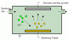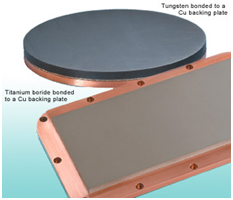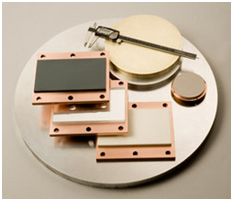
S-Bond soldering is seeing increased application for the solder bonding of sputter targets. Sputter targets are used in a wide range of applications for making thing films used in making electronic chips, solar cells, sensors, TV screens, optical components, electrical devices, and on and on… Sputter targets support a very large physical vapor deposition (PVD) and diverse technological base that is wide ranging and pervasive. Sputter targets under ion bombardment release target material atoms into a high vacuum chamber that under an electric field can be accelerated and deposited onto the component surface where the arriving atoms arrange themselves into a contiguous thin film. Figure 1 schematically illustrates the sputtering process. Ion bombardment is a high energy collisional process that can heat target materials to their melting points unless cooled; hence most sputter targets are bonded to a water cooled backing plate. Backing plates are made normally made from copper and are mounted to a water cooling manifold. Other metallic backing materials are also used. See Figures 2-3 for examples of bonded sputter targets.

To manufacture sputter targets, the target materials, such as W, Ti, Cr, Al, Si, InSnO (ITO), Ce, Ga, Au, Pd, Ag, etc. need to be bonded to metallic backing plate. Soldering or diffusion bonding normally are used since a metallic joint is required in order to provide an electrically and thermally conductive structural joint. The soldering process has been a major bonding technique since soldering is simpler and more versatile and can bond a wider range of materials. For ceramic targets such as Indium Tim Oxide (ITO) and other ceramics and intermetallic targets, Indium solders have used. Indium is a mildly “active” metal that can interact with oxide surfaces and can bond a range of metals without extensive use of flux. Most Sn based conventional solders use flux to clean the backing plate surface and/or the plated target materials, but in the wide bond areas required for many sputter targets, flux is trapped in the interface, later causing contamination in high vacuum sputtering systems. Hence, fluxless soldering is desired. S-Bond and indium solders fit this requirement; however, Indium re-melts at 157°C where S-Bond begins to remelt at 220°C. This increased remelt temperature permits higher power inputs translating to higher sputter rates).
S-Bond solder joining is an active, fluxless process where the Ti, Mg, Ce and Ga in the S-Bond solders enable the solder to interact and wet directly to all metals including Cu, Al, Mo, Ti, W, and Si as well as most compounds and ceramics. Since S-Bond joining requires no plating nor does it use flux, the bonding is direct and complete with no flux filled voids.

As sputter targets get larger and larger for applications such as 300 mm wafers and TV screens, large differences in coefficients of thermal expansion (CTE) make diffusion bonding impossible as cooling from the bonding temperatures distort and many times crack the targets. Soldering is preferred and the lower the temperature of the joining process the better. For conventional soldering of larger targets, Indium solder is preferred when since the lower melting temperature (157°C) of indium and its mildly active nature creates a bond with less CTE mismatch stresses. However, indium solders to lower the power input ratings and lowers the effective sputtering rates. As such, active Sn-Ag solders such as S-Bond can be used to create stronger bonds and higher temperature (remelts at 233°C) target operation.
In the last few years a new bonding process has emerged which improves the solder bonding of large sputter targets that have large CTE mismatch such as CIGS and ITO used in flat panel displays and in solar panels. The process is NanoBond®. It is a “no temperature” process and in combination with S-Bond as a “tinning layer” to wet the ceramics and refractory metals and in combination with Sn-Ag solder, large targets can be bonded. The NanoBond® process using S-Bond is described more fully in another blog article on this website, but in summary, using patented exothermically reactive foils, the heat generated by the preplaced Nanofoils® into bond interfaces that have been pre-tinned with solder, remelts the solder and bonds the target to the backing plated without bulk heating of the target / backing material.
The NanBond® process is sold through the Indium Corporation and they provide bonding services, materials and license their customers to utilize the NanoBond® process in combination with S-Bond solders to make larger sputter targets of widely mismatched CTE materials.
Contact us for more information on S-Bond solders and how we can improve your sputter target manufacturing processes.
NanoBond®; registered trademark of Indium Corporation.
