While it has been several years since manufacturers began moving to lead-free solder procedures, in part due to the European Union’s Restriction of Hazardous Substances Directive, some still believe myths that have long been inaccurate regarding the use of alloy joining materials that do not require flux and are based on lead and tin.
Temperatures Can Be Enough to Destroy Components
The first round of lead-free solder options to join metals and other materials were comprised of tin, silver and copper, which do have a slightly higher melting point of 217 degrees Celsius compared to existing solder’s 183 degrees Celsius. That disparity could cause problems regarding PC board damage.
However, newer products including several offered by S-Bond have significantly lower melting points that make it easier to join metals like aluminum. At the lowest temperatures, some materials can be joined at just 115 degrees Celsius.
Issues Regarding Silicon Will Require Other Materials
S-Bond material joining applications enable engineers to use multiple materials, such as materials and ceramics, in a variety of applications. However, just because aluminum and steel can be joined, as one example, does not mean that the joining process cannot introduce deformations or other issues.
Thermal Expansion Concerns in Bonding
When soldering two different types of metal together, both surfaces have to be heated in order for the solder to bond to both components. Materials expand as they heat, and different metals do so at a different rate. This can create problems as the joining site cools back down.
Two examples of materials that react easily to heat are aluminum and magnesium, which can expand at twice the rate of carbon steel and iron. If an aluminum sheet is soldered to a sheet of carbon steel, during the cool-down period the combined piece will warp with a slight curve. With more brittle components such as those made with ceramics, the combined part can shatter based on expansion during bonding and later cooling.
Solutions for Dissimilar Coefficients of Thermal Expansion
Thermal interface materials are materials used in creating heat conductive paths at interfaces between components and thus reduce thermal interface resistance. These materials permit more effective heat flow between separate components where heat is being generated to a heat dissipation components such as solid state transistors to heat sink or a high frequency device connected to a heat spreader. Thermal interface materials’ purpose is to fill the air gap that occurs at contact interfaces with more thermally conductive compounds to permit more effective heat flow than poorly conductive air.
There is a wide variety of thermal interface materials (TIM’s); thermal greases, phase change polymers, thermal tapes, gap filling pads, filled epoxies and solders. All having various costs, performance and manufacturing challenges.
Figure 1. Illustration of thermal grease filling an interface between a heat generating device and a heat sink.
Thermal greases are viscous fluid substance which increase the thermal conductivity of a thermal interface “gap by filling microscopic air-gaps present due to the imperfectly flat and smooth surfaces of the components as seen in Figure 1.
Thermal grease compounds have far greater thermal conductivity than air (but far less than metals). They are used in electronics, as depicted in Figure 2, to improve the heat flow from lower power electronic devices thus lowering the components temperature and increasing its life.
Bond assembly can be done via 1) mechanical attachment, 2) adhesive bonding of which epoxy bonding is one form of adhesive, 3) soldering bonding using lower melting filler metals (< 450˚C), 4) brazing using filler metals melting above 450˚C and 5) welding such as resistance welding bonding, ultrasonic welding and friction weld bonding that uses locally melted parent metal.
Bonding is done for a variety of technical reasons a) mechanical attachment, b) thermal contact, c) electrical contact d) gas or liquid seal, or e) any of all combinations of a – d. The choice of bonding method will then depend on the intrinsic properties of the bonding filler materials (hermetic, electrical conductance, thermal conductance, thermal coefficient of expansion, adhesive bond strength related to the intrinsic fillers’ mechanical properties and their adhesive and cohesive strengths…
With all these variables and design considerations how does one choose? The three main guiding principles are:
1. Cost of filler and Cost of bonding processes
2. Performance in Service (based on the properties of the bond and bonding materials)
3. Compatibility with Manufacturing Sequence.
To compare epoxy bonds to solder bonds one has to ask the purpose of the bond… Is strictly a mechanical bond ? Is cost a large factor? If cost drives the choice then many times epoxy is the bonding material of choice. Epoxies are generally low cost thermosetting polymers, that are mixed chemicals which are thermally or UV cured to achieve hardness and adherence. Epoxy by far is the lower cost material over solder metal fillers and thus if low cost is the driving aim of the bond, then epoxy will be the bonding material selected. Figures 1-2 illustrate typical epoxy bonded applications
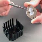
Figure 1. Epoxy bond on heat sink (courtesy of MasterBond®)
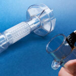
Figure 2. Epoxy seal on tube (courtesy of MasterBond®)
When bonds have to be thermally conductive or electrically conductive solders are usually the bonding material of choice. Solder are metal fillers melt below 450˚C are normally alloys of Sn, Ag, Pb, In, or Bi with the Pb-free alloys being preferred for environmental reasons. As metals, these materials are intrinsically 10 – 100 time more conductive than epoxy bonds. In recent year epoxy bonds have been filled with aluminum or silver particles to increase the epoxy bond filler conductivity to values of 3 – 5 W/m-K from 0.5 – 2 W/m-K. When compared to solder bond metals with conductivities of 40 – 400 W-m-K, one can see for thermal bonded components that solder bonding would be preferred. S-Bond Technologies makes active solder alloys that bond to metals, ceramics, glass and their combinations without the need for flux or plating and are many times selected over epoxy bonds for their improved thermal characteristics. Figures 3 – 4 illustrate typical solder bond applications.
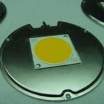
Figure 3. Solder bond LED package to heat spreader. (S-Bond® Technologies)
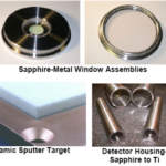
Figure 4. Solder bond seal of windows in housings. (S-Bond® Technologies)
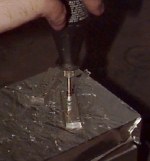
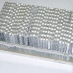
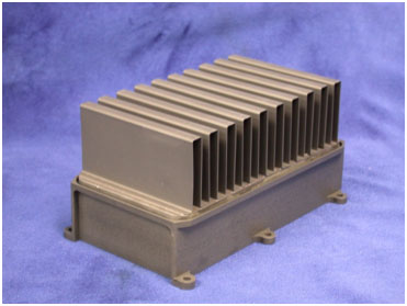
Figures 5-7 show the solder bond process being used to make a heat exchanger.
Figure 5.
Figure 6. Solder bond assembly of heat exchanger. (S-Bond® Technologies)
Figure 7. Final solder bond of finned aluminum heat exchanger. (S-Bond® Technologies)
Bonding for electrical resistance or conductance will many times determine the choice of epoxy bonds over solder or active solders. If the bond joint has to provide electrical isolation, then epoxy has much higher dielectric strength and resistivity, hence are excellent at isolating electrical components from their base materials. However, if the bond has to be electrically conductive solder bonds are preferred.
Bonding for seals are a mixed choice… in the short term epoxy seals can perform and create a sufficient seal for liquids and many gases. However, in applications for long term use epoxy bonds are permeable to certain gases and moisture and are not used in seals that require high hermetic seal integrity. Metals are impervious to moisture and gases thus solder bonds are the preferred bonding materials for high integrity hermetic seals.
Epoxy bonds are “permanent” and less resistant to thermal cycle and temperatures as well as UV exposures (can degrade with time). Solders on the other hand being metallic can be remelted repeatedly to renew or rework the bond. Additionally, as metals, solders are resistant to cracking being ductile and tough and are not susceptible to UV degradation.
Finally, the issue of compatibility with manufacturing sequences and the choice of solder bond vs. epoxy one has to select the bonding materials that will suit not only cost but the sequence of manufacturing operations. The bond has to have the properties that will take the exposure to all the assemblies operations. Bonding is many times completed after machining and fabrication but before plating or coating. If an electrical package the bonding has to be done in a compatible sequence with the electrical soldering operations. For example if a printed circuit board needs to bonded to a heat sink solder bonding the circuit board has to be done a temperatures below the solder reflow temperature on the circuit, for example below 200˚C or one has to epoxy bond the circuit board with a thermally filled epoxy. Compared to solder bonding, epoxy bonds can be less expensive in a manufacturing operation with no need for heating and reflowing solders. On the other hands solders “cure” as soon as the heating is off, while epoxy bonds need “setting time” to cure, which in some high volume applications provide some problems. When electroplating a full assembly, the bonded parts need to be bonded electrically hence solder bonding is the choice, while if powder coating, the epoxy bond may be the bond of choice.
This blog discussed how the choice of epoxy bond vs. solder bond is determined by a host of factors that need to be considered. We hope the discussion has been useful.
If you need help in making the choice of epoxy bond vs. solder please contact us, we can offer the proper counsel for making the right choice and we also offer alternative
Argonne National Laboratories selected S-Bond active solder technology to make water cooled high power microwave beam dump in its Advanced Photon Source which is a user-facility to producing extremely brilliant x-ray photon beams. The Advanced Photon Source uses high energy microwave beams to steer and create such x-ray photon beams. These beams once started cannot be shut down or restarted easily, so to facilitate the use the various beam lines, the microwave beams are diverted to beam dumps. These beam dumps consist of microwave cavities that are lined with SiC tiles bonded to water cooled rectangular copper enclosures that are heavy water cooled. SiC is a well know high efficiency absorber of microwave energy and thus is used in dampers.
The challenge faced by the Argonne engineers and physicists was to find a stable process for bonding the SiC tiles to copper bases that would provide thermal and electrically conductive interface and be able to take the thermal expansion mismatch during the bonding processes and in service. Active brazing and active soldering were considered since active brazes and solders are able to form metallurgical bonds with the SiC tiles. Active brazing, using Cu-Ag-Ti was tested and it was found the residual stresses stemming from the coefficient of thermal expansion (CTE) mismatch of SiC and copper led to the fracture of the SiC tiles upon cooling from the 860˚C brazing temperature to room temperature. S-Bond active soldering was selected as good alternative to active brazing since the solder bonding temperature of 250˚C yielded much lower CTE derived stresses and created a more compliant bond line that would better accommodate the heating and cooling stresses in service.
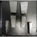
Figure 1 below show the S-Bond joined SiC tiles being bonded into one half of the microwave beam damper cavity indicating how S-Bond successfully joins SiC to copper. Figure 2 is an ultrasonic C-Scan of the bonded interfaces under each tile in the damper half
Figure 1a) SiC tiles with S-Bond solder metallization
prepared to be bonded onto copper bases.
Figure 1b). SiC tiles being solder bonded onto copper bases.
Figure 1c) SiC tiles completely bonded onto
copper bases with S-Bond active solders.
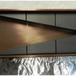
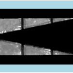
Figure 2) Acoustic C-Scan image of SiC tiles bonded onto copper base
with S-Bond solder. Grey is 100% bonded, white is void at bond line.
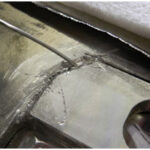
S-Bond Technologies has developed and demonstrated a “solder welding” process that is finding application in the repair of brazed aluminum heat exchangers.
Aluminum heat exchangers and cold plates many times are brazed either by dip brazing or vacuum brazing. In these operations, aluminum braze filler metals are added to joint areas as pastes, brazing foils or braze alloy clad aluminum sheets. Depending on the complexity of the braze joint and the assembly, braze joints can on various occasions after the brazing cycle, be found to leak. Leaks at this point cannot be re-brazed since the aluminum braze filler metals cannot be melted without melting the entire component due to the interdiffusion of the silicon from the filler metal into the base metals. Thus brazed aluminum heat exchangers are normally weld repaired… but with limited success. Many times the weld will “chase” the crack and not seal it and the locally high silicon in the braze joint can also create inconsistent welds and if thin walls are part of the aluminum heat exchanger the high local temperatures from the welding process can “blow” holes in the thing gage. With these limitations on weld repair, solder repair is more viable.
Solder repair is viable since it has low heat input and is conducted below 250˚C, provided the solder filler metal can wet and adhere to the rework areas. Conventional soldering aluminum normally requires Ni-plating and or aggressive fluxes which complicate the rework procedures. S-Bond active solders bond to directly to aluminum and fill in crevices in aluminum surfaces without the need for flux and or preplating, thus it can be used to directly fill machined out leaks on braze joint in aluminum. The process consists of 1) locating leak areas (bubble testing is typically used) 2) grinding out the areas through and adjacent to the leaks, 3) deburring and degreasing the machined areas, 4) heating the plate locally or in its entirety to hold the repair area at 250˚C 5) melt the S-Bond filler active solder with the heat in the heat exchanger 6) spread the S-Bond solder into the joint to mechanically activate the solder to enable it to wet and adhere to the aluminum repair areas. NOTE: is has been found that ultrasonic activation using an ultrasonic solder tip can improve the reliability of the repair soldering process. The figures below illustrate the S-Bond solder aluminum repair on aluminum surfaces.
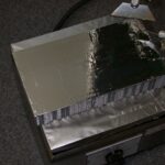
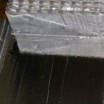
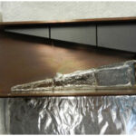
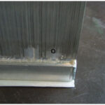
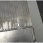
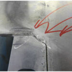
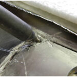
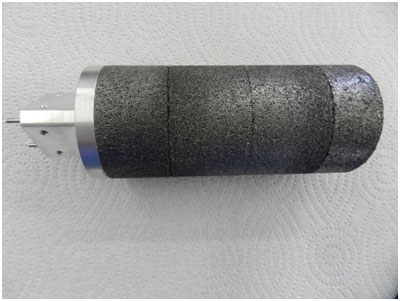
Figure 1a. Multiple plate and fin brazed aluminum heat exchanger
with indicated leak that has been machine out for repair.
S-Bond® active solders are being used extensively as a high conductivity bonding solution for foam cored phase change materials foam cored heat sinks. Increasingly, thermal management in electronics is the limiting factor in performance and/or life of electronics as higher power and higher speed in electronic devices generate more intense heat. High brightness LED’s, high speed/high bandwidth telecommunications, avionics, satellites and solid state conversion devices all have transient and steady power states where intense heat is generated and needs to be channeled away from the electronic device to prevent performance loss or permanent damage. The electronic industry is relying on a host of devices from conventional heat sinks with fins and fans to heat pipes and vapor chambers to more exotic materials and composites that include pyrolytic graphite or diamond. S-Bond materials and processes have been proven to be a good solution when bonding these various components and materials with a metallic “thermal interface material (TIM)” rather than filled polymeric bonding agents.
When electronics have a high transient heat output thermal engineers are using “phase change” heat sinks. Such heat sinks utilize “phase change materials (PCM’s)” that when exposed to heat absorb it very quickly and effectively as the material “changes phase”… either going from solid to liquid or liquid to vapor. Materials with high latent heats of fusion or latent heat of vaporization at or near the maximum temperatures that electronics are being used in the core of such heat sinks. In PCM heat sinks during the phase change there is the potential to rapidly absorb a high heat load… that can later be more slowly released to the atmosphere with cooling fins as the phase change is reversed and the heat is released away from the electronic device.
Two of the most used PCM’s are paraffin and water… each has a high latent heat of fusion or heat of vaporization, respectively. The challenge in the use of PCM’s is to overcome their relatively low thermal conductivities. For example, in heat sinks with paraffin as the PCM, when the heat transfers from the electronic device into the heat sink package, the outer layer of paraffin melts and then slows the transfer of heat into the solid paraffin core. To offset this heat flow limitation, designers are incorporating metallic or graphitic foams into the core of the heat sinks. The foams’ cells separate the PCM’s into small reservoirs that are surrounded by high thermal conductivity cell walls that then transfer the heat to a small PCM filled pore in the foam and therefore quickly melts the paraffin or vaporizes the water. Later in the “reverse” cycle, the conductive foam “cell walls” transfer the heat out of the PCM filled pores to solidify or condense the full volume PCM in the heat sink.
S-Bond joining has found excellent application in paraffin based PCM heat sinks in combination with graphitic foams (PocoFoam® or K-Foam®). S-Bond can effectively bond to graphite and graphite foams to heat sink package materials such as aluminum, copper and many heat sinks composites such Al-SiC, Al-Gr, Cu-W or Cu-Gr. In such graphite core/paraffin heat sinks. S-Bond Technologies has S-Bond metallized the Gr-Foam preparing for it to be soldered directly to the heat sink package. After S-Bond metallization, various S-Bond solders and processing can be used to bond the graphite foam to the components of the heat sink.
Figure 1 shows a PCM core finned Aluminum heat sink box used to cool high power laser diode packages mounted on the flat side opposite the side with the fins. The aluminum box contains a core of graphite foam bonded to the walls and base of the aluminum enclosure. The aluminum enclosure is then heated to 100˚C and filled and infiltrated with paraffin PCM’s. After filling the enclosure is sealed and the assembly is a PCM heat sink. When the laser diodes are on for intermittent periods of time the graphite foams thermally bonded to the wall of the enclosure heat the PCM… later when the heat load from the diodes are off, the bonded fins with air convection assist, cool and solidify the paraffin PCM to get the heat sink ready for the next thermal cycle. S-Bond active solder joining enabled the graphite foam to have an excellent thermal interface to the enclosure without filling the graphite foam and compromising the graphite foam’s ability to hold and transfer heat quickly to the paraffin PCM.
Figure 2. Graphite foam cored PCM heat sink for hot fluid channeled into the core.
Figure 2 shows another type of PCM cooling. The alternating bonded fluid circulating aluminum tubes bonded with S-Bond sandwiched between S-Bond metallized and bonded graphite foam plates. The stack is later encased in an enclosure and paraffin PCM is infiltrated into the foam to make a large ~ 24” x 24” x 12” PCM heat sink. When heated fluids circulate in the aluminum tubes the PCM filled graphite foam core rapidly absorbs the heat from the fluid.
Figure 3 illustrates another style of PCM heat sinks that are mounted around a central heat pipe. In this design, S-Bond metallization of the faces and ID’s of the graphite annular rings permitted a graphite foam outer core to be become an effective PCM heat sink for a heat pipe cored thermal management device.
Contact us to evaluate how S-Bond can be used to enable your thermal management components to be made and how phase change material (PCM) heat sinks can be effectively incorporated into your designs.
Figure 1. Typical thick film heater. (Heatron website)
“Thick film” heaters are built from conductive, resistive, or dielectric circuit elements that are deposited via screen printing materials (~0.0005″ thick) onto substrates. Thick film are made from inks made by mixing ceramics and metals (known as cermets) to make the resistors and conductors.
Figure 2. Image of mechanical attachment for thick film heater (Watlow website)
Typically the metallic materials are silver, gold, platinum, palladium, ruthenium and related alloys. Glass-ceramic inks are also used for dielectrics between encapsulants covering the circuit layers. Substrates include steel, stainless steel, alumina and more aluminum nitride.
Figure 3. Picture of patterned thick film heater with soldering pads
The challenge is to make reliable solder connections that perform at thick film heater temperatures (200 – 350°C) and eliminate more expensive mechanical connections, as shown in Figure 1 – 3 . S-Bond Technologies has developed and patented active solder S-Bond® 400. S-Bond 400 Zn-Al-Ag-Ce alloy that can, with mechanical activation, bond electrical leads without plating and/or flux, to many of the various commercial heater elements as shown in Figures 4 – 5.
Figure 4. S-Bond 400 bonded terminals on AIN base heater
Figure 4 illustrates S-Bond 400 active solder joints that were produced by ultrasonically soldering “pre-tinned” copper wire leads to pads on heater substrates. The process consists of first stripping the high temperature insulation back from the wire lead, heating the leads to 450°C with hot air, adding S-Bond 400 solder to the tip of an ultrasonically activated solder iron, and tinning the wire lead. After tinning the leads, the thick heater substrate is heated and the ultrasonic soldering iron tip presses the S-Bond 400 tinned lead to the thick film pads on the heater.
Figure 5. S-Bond 400 bonded copper terminals on base heater.
The S-Bond 400 joints permit the heaters to operate at higher temperatures with a direct solder joint, not a mechanical connection and produces stronger connections than conventional solder joints since the Zn-Al-Ag-Ce alloys do not soften until well above 300°C. Additionally the flux free joining process eliminates the contamination that fluxes can cause and also eliminate the need to post solder clean.
Conventional soldering processes use chemical fluxes to remove the oxides from the molten filler metal and the underlying base metal surfaces that are being solder joined. In these processes, once the oxides are removed from the molten filler and the base surfaces, the molten filler wets and form a metallurgical bond. The problem with chemical fluxes is that they are corrosive chemicals and in any flux residue on the surface there is the potential of corrosion which is a long term reliability problem. Ultrasonic soldering is process solution that removes the need for corrosive chemical fluxes.
Figure 1 illustrates the ultrasonic soldering process mechanism employed a heated solder probe tip which is vibrated at frequencies from 20 – 60 kHz. Focused acoustic power in the specially designed tips initiates cavitation in the molten solder which remove oxides at the surface of the molten filler metal and at the surfaces of metals being joined. The molten solder acts as the acoustic transfer medium for the ultrasonic energy and as cavitation ( micro-bubbles) burst on all surfaces the action cleans the surfaces and exposes oxide-free metal that is immediately wetted by the surrounding molten filler metal.
Figure 2. Picture of ultrasonic soldering station from MBR Electronics
Figure 2 illustrates a typical commercially available ultrasonic soldering iron. One should note that ultrasonic soldering is not ultrasonic welding. Ultrasonic welding (bonding) employs higher pressure shear forces and does not have molten metal phase and is a high frequency shear force micro-friction welding process.
Figure 3. Ultrasonic solder wetting on glass
Ultrasonic soldering is very well suited as a mechanical activation process for fluxless soldering with S-Bond active solders. S-Bond solders rely on reactive elements such as titanium (Ti) and rare earth elements such as Cerium (Ce) to enable direct wetting of metals, ceramics and glass without the need for chemical fluxes or plating. However, active solders are not “self” wetting since their own oxides that form on melting create a barrier to the reactive elements in the molten solder. The cavitation from an ultrasonic solder iron tips disrupt these oxide films that form on the molten solder. Figure 3 illustrates how an ultrasonically activated heated tip enables the active solder fillers to wet and adhere directly glass. The same process enables active solders to wet and bond to works on all metals and ceramics.
Figure 4. Ultrasonic soldering along a line. (Japan Unix)
Ultrasonic soldering tips can be narrow and suited for soldering narrow lines and/or point soldering as shown in Figure 4, or larger heated ultrasonic horns (Figure 5) can be used to activate a much larger area to deposit an active solder layer as the first step in soldering two surfaces together with an active solder.
Ultrasonic soldering of active solder is an excellent high volume production process. Figure 6 illustrates a wire fed robot operated soldering iron that can be used in spot, line or large area ultrasonic activation of active solders.
Ultrasonic soldering is growing in application with the ever increasing use of dissimilar materials and where many soldered assemblies need to eliminate the use of corrosive and contaminating fluxes. Also ultrasonic soldering and active solder permit the precise placement of solder filler metal.
Piezoelectric sensors stem from the natural effect in certain crystals that generate a voltage when the crystal is deformed. A piezoelectric sensor uses the piezoelectric effect to measure pressure, acceleration, strain or force by converting them to an electrical charge, as illustrated in Figure 1. Such sensors are used in medical, aerospace, nuclear instrumentation, and as a
Figure 1. Illustration of piezoelectric effect
pressure sensor in the touch pads of mobile phones. In the automotive industry, piezoelectric elements are used to monitor combustion when developing internal combustion engines. The sensors are either directly mounted into additional holes into the cylinder head or the spark/glow plug is equipped with a built in miniature piezoelectric sensor.
Two main groups of materials are used for piezoelectric sensors: piezoelectric ceramics and single crystal materials. The ceramic materials include PZT (lead zirconate ceramic) and new single crystal materials such as Lead Magnesium Niobate-Lead Titanate (PMN-PT).
The challenge when making sensors is to make an electrical connection to the crystal and also to bond the crystal to the sensor elements and housing. Many times these piezoelectric crystals are silver or gold coated on their attachment surfaces to which conventional solder joints can be made to make electrical and mechanical connection; however many times these solders introduce fluxes or require plating. Active solders such as S-Bond can, with their reactive elements, directly bond to the crystal surfaces without the need to initially coat the crystal surfaces. Also, S-Bond Technologies range of active solders, bond at temperatures from 115 – 400°C. These active solder alloys permit the bonding of the piezoelectric crystal well below the crystals’ Curie temperature, where these crystals lose their piezoelectric properties.
Figure 2 shows an S-Bond 220 joined PZT crystal, bonded to an aluminum housing. This bonded assembly is part of an ultrasonic actuator.
Figure 2 PZT crystal S-Bond soldered to aluminum housing.