215.631.7111

S-BOND BLOG

Ultrasonic Assisted Solder “Welding”
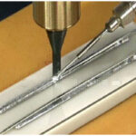
Fluxeless Ultrasonic Soldering
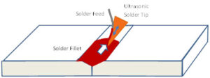
Figure 1. Ultrasonic soldering along a line. (Japan Unix)

S-Bond Technologies have demonstrated a process for making “active solder filler metal” joints and seals on aluminum assemblies. The process is similar to MIG welding processes which use higher melting temperature filler metal wires fed into a moving arc to create a weld fillet. In Ultrasonic Assisted Solder “Welding”, an ultrasonic solder tip is a heat source to melt the solder wire, instead of a welding arc. The heated tip melts S-Bond 220 wire solder which is continually fed to the solder tip, as seen in Figure 1. For aluminum soldering it is suggested the area of the joint be heated to the solder melting temperature using supplemental heat sources to provide a stable molten pool for the ultrasonic activated tip to run.

The solder iron tip is “drawn” through a molten solder bead on the heated aluminum component faying surfaces (190 – 250C) in order to deposit a solder bead that through mechanical activation wets and adheres to the underlying aluminum. This ultrasonic assisted technique enables the active S-Bond solders to directly wet and bond to the underlying aluminum surfaces without the need for an aggressive chemical flux.

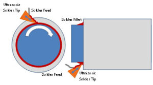
Figures 2 and 3 illustrate the Ultrasonic Assisted Solder “Welding” process on a tube enclosure and on butt joint for aluminum sheet. In these applications the component surfaces are heated and the active solders are melted and applied via the heated soldering iron tip to form a molten bead at the joint. The ultrasonic soldering iron tip is submerged in the bead and mechanically disrupts the oxides on the active S-Bond solder. Due to the active elements in S-Bond, the ultrasonic gitation of the solder tip enables the solder to directly wet and adhere to aluminum and many other metals.

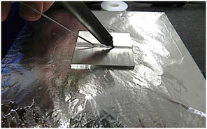
Figure 4 shows an actual Ultrasonic Assisted Solder “Welding” process in operation as it forms a joint between two aluminum sheets.
ultrasonic soldering with S-Bond solder wire fed to U/S soldering iron tip
Figure 2. Illustration of a tube enclosure being sealed via ultrasonic soldering with S-Bond solder wire fed to U/S soldering iron tip.

aluminum plates being joined via ultrasonic soldering
Figure 3. Illustration of two aluminum plates being joined via ultrasonic soldering with S-Bond solder wire fed to U/S soldering iron tip.

aluminum plates being joined via ultrasonic soldering with S-Bond solder wire fed to U/S soldering iron tip.
Figure 4. Picture Ultrasonic Assisted Solder “Welding” of two aluminum plates being joined via ultrasonic soldering with S-Bond solder wire fed to U/S soldering iron tip.
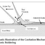
Illustration of Cavitation Mechanism in Ultrasonic Soldering
Figure 5. Illustration of U/S soldering.

Figure 5 illustrates the mechanism of how an ultrasonically activated heated tip enables the active solder fillers to directly bond to most metals. The figure illustrates how an ultrasonic soldering tip creates cavitation (intense bubbles) in the molten solder which disrupts oxides that have formed on the molten solder and the joint surfaces. The cavitation in effect, cleans and mechanically fluxes the soldering area. The soldering tips are driven by a power source that excites the ultrasonic soldering horn at 12 – 25 W of power and a transformer to resistively heat soldering iron tip. Figure 6 is a picture of typical ultrasonic soldering equipment.


Ultrasonic soldering is very well suited as a mechanical activation process for soldering with fluxless, active solders such as S-Bond. S-Bond solders rely on reactive elements such as titanium (Ti) and rare earth elements such as Cerium (Ce) to enable direct wetting of metals, ceramics and glass without the need for chemical fluxes or plating. Ultrasonic “solder welding” is an extension of this principle that can be used to make joints and seal in aluminum assemblies without
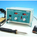
Ultrasonic Soldering Station from MBR Electronics
Figure 6. Picture of ultrasonic soldering station from MBR Electronics

having to use conventional aluminum welding which might distort or “burn though” thinner aluminum structures.Active solders are versatile at joining and sealing many different types of assemblies. Ultrasonic solder welding is another example of how S-Bond Technologies adapts processes to provide bonding solutions.


Contact us to evaluate how ultrasonic solder welding or our other bonding solutions can be used in your applications.

S-Bond Technologies “Industry News” Webpage

S-Bond Technologies has added a News section to its website. This news section is focused on industry and technology developments that may be of general interest to you or may impact your business. Our Industry News feed will be updated during each month as targeted technology and industry news is identified.  Dr. Ronald Smith, President of S-Bond Technologies says “Our Company is materials technology focused with solutions in metals and ceramic bonding that are well suited for dissimilar materials joining, aluminum bonding, and ceramic to metal bonding. Applications for our technology include thermal management, alternative energy, sensors, electronics, aerospace and automotive. We are providing this Industry News section focused on applications that benefit from bonding technology as a feature for our website visitors and customers.”

This industry news provided at our website www.s-bond.com centers on materials technology in industry where bonding/soldering/brazing challenges are prevalent. The News section articles will be available in an S-Bond News Team periodic email that will feature the most recent news articles.

Please if you want to opt-in on our periodic S-Bond News Team communication… please click the link below. If you do not opt-in, you can still see the news by visiting our website, www.s-bond.com . If you do not opt-in, you will remain on our S-Bond e-Newsletter that features S-Bond related technical articles.

Opt-In for the S-Bond News Team communication.

New Lower Temperature Active Solders Developed

S-Bond Technologies has developed and proven a new, lower temperature active solder that melts from 135 – 140°C. The solder, S-Bond® 140 is based around the Bismuth-Tin (Bi-Sn) eutectic composition. This new solder is a lower temperature active solder that enables multi-step soldering where previously soldered connections/seals are not remelted. Active solders that melt below 150C are also finding use in thermally sensitive applications where Sn-Ag based solders that melt over 215°C can thermally degrade the component parts being assembled. Lower temperature soldering also can more effectively bond dissimilar materials where thermal expansion mismatch many times fractures or distorts an assembly’s component parts.

S-Bond 140 is already finding application in glass-metal seals in electronic packages where higher temperature soldering alloys would have damaged the packages’ components. S-Bond 140 is also being used to bond heat pipes and vapor chamber thermal management devices to protect the thermally sensitive phase change fluids from damaging the devices when solder bonding to electronic and LED devices.

Electro-optical package to be bonded to heat sink with S-Bond® 140

Joining of Heat Pipes and Vapor Chambers

Figure 1. Illustration of vapor chamber heat spreader with CPU heat source

Heat pipes and vapor chambers are used to transfer and/or spread heat from concentrated heat sources such as high brightness light emitting diodes (LEDs) and high computing speed CPUs. These active thermal management devices are enclosures/tubes that have porous wick materials lining the walls that provide condensation surfaces and small connected pores that via capillary force, transfer condensed fluids that were originally vaporized at heat source surfaces. When the vapor is transported via convection to the cooler surface to condense, the fluid is then channeled back to the heat source surfaces in a continuous cycle, in effect pumping the heat out of the package without using external power surfaces. Figure 1 illustrates a vapor chamber used to cool a mounted CPU.

Figure 2. Light emitting diode package bonded to vapor chamber

Thermal management is critical in the life and performance of such electronic components that all employ a variety of thermal interface materials (TIMs). With increased power and speed, the polymer-based TIMs being used today are limiting and metal bonding with solders is growing in application. Conventional Sn-Ag soldering temperatures can overheat the thermal fluids in heat pipes and chambers while Indium (In) solders are expensive and do not bond as well as active solders. Responding to this need, engineers at S-Bond® Technologies have announced its latest alloy, S-Bond® 140 as an effective TIM for bonding CPUs or LEDS to heat pipes and vapor chambers.  The Bi-Sn-Ag-Ti alloy can wet and join to all metals including aluminum and to most ceramics and glasses.  S-Bond® 140 is lead free, does not require plating and flux thus keeping electronic and LED packages clean.

Figure 3. S-Bond 140 bonded heat pipe assembly

Figure 2 illustrates a high brightness LED array that has been bonded to a Ni-plated copper vapor chamber with S-Bond 140 solder. This technique provides a high strength and high thermal conductivity metallic solder bond. Figure 3 is another example showing S-Bond 140 solder bonding copper heat pipe tubes (water as the phase change fluid) into aluminum slots to enhance the cooling from the heat pipe to the aluminum package base without plating and flux.. Normally when soldering heat pipes over 200°C, the water in the heat pipe goes to vapor and the resultant pressure distends/distorts the thin copper tube walls. Lower temperature metallic solders, such as S-Bond 140.

Contact us for more information and to order our S-Bond products.

Design Considerations for Solder Bonding

Solder bonding is a versatile lower temperature bonding process that is used in joining a range of metals, ceramics, glass and metal: ceramic composites. By definition, solders are joining filler metals that melt below 450°C. Solder bonding is typically used in the assembly of structures for its good thermal and/or electrical contact or for creating seals. The advantage of solder bonding stems from lower temperature exposure (less that 400°C), compared to brazing when joining thermally sensitive materials.  Alternatively, compared to bonding with epoxy adhesives, solder bonding is a more conductive bond, but does require higher temperature exposure and the wetting of the molten metal to the bonding surfaces.

Figure 1. S-Bond joined heat pipe assembly bonding copper pipes to aluminum base

Because of it excellent thermal and electrical conductivity, solder bonding finds application in the manufacture of sputter targets, heat spreaders and cold plates and other related thermal management components. Solder bonding is also used to seal ceramic:metal and glass windows used in optical based sensors and in other fluid cooled enclosures.  Figures 1 and 2 show several typical solder bonded parts.

Solder bonding (e.g. S-Bond®), despite being versatile and capable of joining most materials, one must consider several issues when active solder bonding…

  • Thermal expansion mismatch
  • Size and shape of bonded parts
  • Interaction with post solder bond processing
  • Galvanic corrosion coupling
Figure 2. Aluminum to copper cooling tubes and ceramic to plated copper sputter targets.

In every application being evaluated for a solder bonding solution, the component and process design needs to consider the following issues.

  • Minimize CTE mismatch of bonded materials to prevent distortion or fracture.
  • Understand post bonding processes to prevent damage of bond interface.
  • Know Service Temperature and Thermal cycling effects on bond interface.
  • Understand effects of service environment on bond interface corrosion

Thermal expansion mismatch (CTE): solder bonding requires heating the component parts in an assembly to 120 – 400°C, depending on the solder filler metal being used.  When similar materials are being joined there is no CTE mismatch so it is not a concern. However; many times solder bonding is being used to lower the CTE mismatch… but despite the lower bonding temperature, it is not alone a “silver bullet” universal solution. Even when heating to 250°C, melting for Sn-Ag based solders, upon cooling once the solder solidifies it can transfer a strain. Then the CTE derived stresses can distort metal assemblies, fracture a glass or ceramic components or fracture the bond. Thus, one needs to minimize CTE mismatch stresses by selecting assemble component materials that are as close as possible in CTE.

When matching CTE is not practical, then one should design the component parts with size and thickness in mind… larger bond areas will “accumulate” more stress and lead to more distortion and/or fracture. A solution for larger parts is to “tile” the component parts; by tiling (mosaic) the strain mismatch accumulation is interrupted and lower the accumulation of stress in the assembly.

Post solder bond processes such as post solder bond heating either with another solder process, welding or bake outs to dry or cure components. Coatings may also be required on a bonded assembly where the heat and or chemical exposure of the coating process, as in electro-plating (see the coating blog article), interacts negatively with the solder bond.

When post processing a solder bonded part, temperature exposures typically should be below 90% of the solidus temperature (temperatures where solder alloys begin to melt) to maintain the bond. The thermal cycle itself can be damaging to the bond, even if the temperature is below this limit, especially with assemblies that have dissimilar materials. The processes that can degrade solder bonds include, other solder steps, welding, bake out or curing, and coating. Therefore; one needs to understand their impact on the solder filler metals and the solder bond interface.

Service conditions can also limit the performance and life of solder bonds. Temperature in service generally needs to be restricted to be below 80% of the solidus temperature of the solder filler metal (although active solders such as S-Bond® can be used up to 90%) to maintain sufficient bond strength. Thermal cycles are more damaging than constant temperature exposure and can be more damaging when CTE mismatched materials. Joint design can mitigate some of these effects by…

  • Selecting component materials to lower CTE mismatch
  • Minimizing area of solder bond and consider tiling, if practical
  • Using thicker cross sections, if possible,  to limit distortion
  • Orienting or mechanically supporting solder bonds/seals to lower bond stresses.

With proper design solder bonded assemblies can be superior to epoxy bonded joints and work very well and compete with brazed or welded joints

Contact us for more information and to order our S-Bond products and Services.

S-Bond® Solders At the Interface of the NanoBond® Process

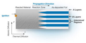
Figure 1. Illustration of the NanoBond® / NanoFoil® heating process® (from www.indiumcorp.com)

S-Bond active solder layers have been shown in many applications to be the key ingredient that permits many ceramics and refractory metals to be bonded to largely coefficient of thermal expansion (CTE) mismatched metals such as aluminum and copper. Indium Corporation offers a NanoBond® process that uses NanoFoil ® as local heat source to remelt preplaced solder layers without the need for the bulk heating of assembled components that have large CTE mismatch. Active S-Bond solders are applied as prelayers and have Ti, Ce, Ga and Mg additions that permit them to wet any ceramic or metal surface. Once the S-Bond pre-layers are applied to ceramic and/or metallic surfaces, conventional solders can be reflowed onto the S-Bond layer to create the preplaced solder layers that are remelted and bonded via the heat emitted from an ignited NanoFoil®. Figure 1 illustrates how temperatures of over 1,400 K are generated by an ignited nano-engineered foil. (more…)

S-Bond Joining of High Brightness LEDs

S-Bond active solder joining is emerging as an effective method to bond heat sinks to the back of High Brightness Light Emitting Diodes (HBLEDs). Active solders can wet and adhere to many of the thermally conductive ceramics (AlN, BeO, etc.) that are being used in HBLED’s and enable effective and thermally stable and conductive joints. (more…)

Fluxless Soldering of Sputter Targets

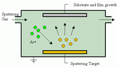
Figure 1. Schematic of sputtering process

S-Bond soldering is seeing increased application for the solder bonding of sputter targets. Sputter targets are used in a wide range of applications for making thing films used in making electronic chips, solar cells, sensors, TV screens, optical components, electrical devices, and on and on… Sputter targets support a very large physical vapor deposition (PVD) and diverse technological base that is wide ranging and pervasive. Sputter targets under ion bombardment release target material atoms into a high vacuum chamber that under an electric field can be accelerated and deposited onto the component surface where the arriving atoms arrange themselves into a contiguous thin film. Figure 1 schematically illustrates the sputtering process. Ion bombardment is a high energy collisional process that can heat target materials to their melting points unless cooled; hence most sputter targets are bonded to a water cooled backing plate. Backing plates are made normally made from copper and are mounted to a water cooling manifold. Other metallic backing materials are also used. See Figures 2-3 for examples of bonded sputter targets. (more…)

Soldering Silicon Carbide (SiC) for Electronics and Optics

Figure 1. Steel fitting S-Bond joined to SIC

S-Bond active soldering of silicon carbide (SiC) has recently been demonstrated on a range of electronic and optical components, providing for metal to SiC joints in plug, mounting and/or water cooling fittings. Silicon carbide is ceramic semiconductor with good thermal conductivity (120 W/mK) and low thermal expansion ( 4 ppm / °C). Thermal conductivity is comparable to aluminum with 1/8 of aluminum’s thermal expansion coefficient (CTE), making it a very stable material. The manufacture techniques for SiC and Si:SiC have recently developed to permit more complex SiC based components. As a ceramic, SiC is very difficult to machine so normally powder sintering and infiltration and/or slip casting and sintering followed by infiltration is used making for making complex shapes. Because of its thermal, electrical and optical properties, SiC and SiC composites are seeing increased industrial application in electronics and optics thus driving an interest for robust SiC joining methods. For high temperature SiC applications vacuum active brazing has proven effective; however, for lower temperature electronic and optical applications, there has been interest in solder joining methods. (more…)

Ultrasonic Soldering & Active Solders

S-Bond® active solders are very effective in combination with ultrasonic soldering for a range of applications. Ultrasonic soldering (U/S) is a fluxless soldering process and is finding growing application in soldering of metals and ceramics from solar photovoltaics and medical shape memory alloys to specialized electronic and senor packages. U/S soldering has been reported since 1955 as a method to solder aluminum and other metals without the use of flux. The reason for expanding usage is that ultrasonic soldering is a fluxless process. (more…)