215.631.7111

S-BOND NEWS

IME Forms Chip-On-Wafer Consortium

Chip-on-wafer technology
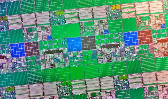
Chip-on-wafer technology could pave the way for higher-performance, slimmer and more cost-effective electronic devices.

Conventional Chip-on-Wafer bonding techniques used for making 3D chipsets rely on a solder-assisted thermo-compression bonding process that takes more than 15 seconds at a minimum of 300 degrees Celsius to complete. This method, which attaches the chip to a piece of semiconductor wafer, slows the overall production process and results in higher manufacturing costs.

AsianScientist (Dec. 29, 2014) – A*STAR’s Institute of Microelectronics (IME) has formed a Chip-on-Wafer (CoW) Consortium to enable semiconductor firms to develop commercially-viable capabilities for making 3D chipsets.

The consortium is working on overcoming such challenges by using low temperature copper-copper (Cu-Cu) diffusion bonding.

Read more at: http://www.asianscientist.com/2014/12/academia/ime-forms-chip-on-wafer-consortium/

Building the Next Generation of Efficient Computers – Multiferroic Materials

As wireless and mobile systems advance, thermal management technologies will be crucial to their development.

Bryan Huey, a UConn researcher, has uncovered new information about the kinetic properties of multiferroic materials that could be the key breakthrough scientists have been looking for to create a new generation of low-energy, highly efficient, instant-on computers.

Materials known as multiferroics have shown great promise for creating a low-energy memory storage and processing device because they have the rare ability to be both magnetic and ferroelectric, meaning they can be sensitive to magnetic and electric fields simultaneously.

The findings were featured in the Dec. 17, 2014 issue of Nature, considered one of the world’s most prestigious scientific research journals.Read more at: http://today.uconn.edu/blog/2015/01/building-the-next-generation-of-efficient-computers/

How GM Will Use Multiple Aluminum Joining Technologies in the New Cadillac

Multiple Aluminum Joining Technologies in the New Cadillac
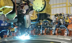
In manufacturing engineering, the search for the “best way” to fasten components into subassemblies is a major part of the job. There are lots of options, spot welding has been the method of choice for decades.

Now that aluminum is becoming the preferred unibody construction material, General Motors is using a novel mixed approach to building the new Cadillac CT6 large sedan.

The Cadillac CT6 will use 7 different ways to join body parts.

Low-cost aluminum joining technologies could make lower volume sub-assemblies more economical.

“Never before has an automaker brought this combination of joining techniques together for a single vehicle,” said Travis Hester, CT6 executive chief engineer. “The manufacturing team has enabled body engineers to optimize the vehicle for mass, safety, stiffness and materials with more precision than ever.
Read more at: http://www.engineering.com/AdvancedManufacturing/ArticleID/9468/How-GM-Will-Use-Multiple-Aluminum-Joining-Technologies-in-the-New-Cadillac.aspx

Popular aluminum oxide created by interlacing different crystal forms

Bonding Aluminum OxideYour automobile exhaust system, the plastic cup holding your favorite drink, along with many, many other products, rely upon chemical reactions driven by catalysts supported on aluminum oxides. Characterizing these aluminum oxides or alumina has been challenging. Now, scientists at Pacific Northwest National Laboratory (PNNL) and FEI Company obtained an atomically resolved view of the alumina form known as delta alumina. Using experiments and computational approaches, the team showed that the oxide is made up of two crystal forms or variants woven together.

As researchers continue to characterize the structure and behavior of delta alumina and its related polymorph, gamma alumina, “the materials present a lot of questions,” said Dr. Libor Kovarik, PNNL scientist and lead author on the study. “We are working to understand them, particularly the aluminum bonding on the catalysts surface.”

Read more at: http://phys.org/news/2014-11-popular-aluminum-oxide-interlacing-crystal.html

Aluminum Soldering Plays Key Role in NASA’s Mars Missions

Mars probe uses advanced aluminum soldering

While everyone was watching the Mars Curiosity Rover as it landed delicately on the surface of the red planet and explored its surroundings, other NASA projects have focused on analyzing the atmosphere and obtaining other data. Without aluminum soldering as part of creating composite structures, none of that would be possible.

MAVEN (Mars Atmosphere and Volatile EvolutioN) will not reach its expected orbit around Mars until September, but it is already an example of the efforts to create long-lasting chassis to handle rough landings and other extreme conditions. The frame is made of aluminum sheeting with composite materials in between the metal materials and is based on advancements of joining these materials pioneered by the supercar industry to improve safety of drivers and their passengers. (more…)

Copper Pricing and Why Metal Joining Could Be Affected

Raw materials costs can quickly make it difficult for companies to maintain their profit Sonic Solder-Bonding Dissimilar Materialsmargins on a given product. At a time when copper prices have been steadily increasing, it may make sense for firms to look at other materials. Yet to do so, they may also need to consider alternatives to achieve dissimilar materials joining.

Companies in China are moving from using copper in cabling to using aluminum, a Metal Bulletin report indicates, where just 10 percent of total production uses the metal compared to roughly 50 percent in the U.S. and even more in other developed countries. The rationale is that the cables can be priced 20 to 30 percent cheaper due to the decrease in material costs. Similar moves are occurring throughout the electronics industry. Yet without the use of specific metal solders to join materials, adapting designs can be extremely difficult.

(more…)

Skyrocketing LED Market Will Require Extensive Lead-Free Solder Development

A recent market research report estimates that the solid-state lighting market that produces light-emitting diodes (LEDs) will reach roughly $57 billion by 2018 as a result of consistent double digit growth. While the industry has made significant inroads in the commercial sector, further developments in design using disparate materials joining will be necessary to make an impact in the residential lighting field.

By January 1, 2014, nearly every incandescent light bulb will be off the market due to federal regulations. The current standard is compact fluorescent bulbs, but LED light bulbs are also making inroads. Currently, companies like Cree and Philips subsidiary offer luminaires that look like light bulbs, but the cost savings require homeowners to have them installed for years. The goal to reduce costs will rely in part on Haitz’s Law but moreover on improved product designs with the use of lead-free solder.

Haitz’s Law is a formula estimating that the cost per lumen, or light output will be one-tenth of what it was a decade earlier, while output will jump a similar amount. However, the designs of standard and organic LEDs (OLEDs) require large heat sinks in order to dissipate heat at the junction where light is created.

New solder materials and developments in the technology will likely reduce these requirements, but this must be done relatively quickly in order to meet the Markets target of 25 percent compounded annual growth for OLEDs. Competition is already fierce for applications like TVs, commercial lighting for storage facilities and parking lots as well as backlighting applications.

The last market that will be up for grabs for is both low-cost lighting assistance for screens as well as light bulb replacement options as the cost approaches that of compact fluorescent bulbs and families are unable to buy incandescent bulbs. Innovations are likely to come both from efforts to lower costs of industrial applications as well as work on shrinking backlighting for consumer electronics.

For more information on the Markets for Markets research, visit http://www.marketsandmarkets.com/Market-Reports/solid-state-lighting-market-1234.html

A Better Heat Sink: New Ways To Dramatically Increase Thermal Dissipation

Heat Sink - S-Bond Technologies It’s common knowledge that slapping a better heat sink, water cooler, or phase-change unit on a CPU can yield better overclocking results, but there’s more to the CPU cooling issue than simply bolting on a better heat sink. One of the biggest barriers to higher CPU clock speeds is hot spots.


So how do you fix that?

There are a few proposed methods. One alternative is to boost the efficiency of the thermal interface material (TIM). Intel has caught flack in recent years for using thermal paste, not solder, for its microprocessors. Another option is to improve lateral heat transfer within the CPU itself. Other approaches, like computational sprinting, could be combined with new phase change materials like wax to dramatically increase thermal dissipation for short periods of time.

Another solution to the heat issue is to adopt new materials. Certain element combinations from Groups III and V of the Periodic Table are well suited to high-frequency, low-voltage operation.

There’s a third idea out there that’s attracted significant interest in recent years. Why not leverage the advantages Moore’s law still offers to build fundamentally different kinds of chips?

Click here to view the full, original article “Post-post-PC: The new materials, tech, and CPU designs that will revive overclocking and enthusiast computing.”

S-Bond Announces New Ultrasonic Assisted Solder Welding

Ultrasonic Assisted Solder Welding: S-Bond S-Bond Technologies has developed an ultrasonic assisted soldering process for making active solder filler metal joints and seals on aluminum assemblies. The process is similar to MIG welding processes in which filler metal wires are fed into a moving arc to create a weld fillet. In Ultrasonic Assisted Solder “Welding”, an ultrasonic solder tip serves as the heat source to melt the solder wire, instead of a welding arc. The heated tip melts S-Bond 220 wire solder which is continually fed to the solder tip. S-Bond active solder alloys melt at lower temperatures than the filler metals used in traditional MIG welding. Lower bonding temperatures are just one of the many processing advantages realized with Ultrasonic Assisted Solder Welding.

Ultrasonic Assisted Solder Welding Dr. Ronald Smith, President of S-Bond Technologies reports, “This solder-welding process will enable the sealing of thin aluminum sheets where normal MIG or TIG welding would burn through the aluminum because of its low melting temperature. S-Bond has successfully proven this process as an alternative for aluminum bonding applications.”

For more information on S-Bond Ultrasonic Assisted Solder Welding, please contact S-Bond Technologies at (215) 631-7114 x 102 or email [email protected].

S-Bond Develops New Lower Temperature Active Solder Alloy

Solder Alloy- S-Bond 140 AlloyS-Bond Technologies has developed S-Bond® 140, a new, lower temperature active solder that melts from 135 – 140°C. This new alloy is formulated with a Bismuth-Tin (Bi-Sn) eutectic base composition, which is then alloyed with active elements and rare earths.  The resulting S-Bond® 140 active solder successfully bonds a wide range of materials without the requirements of flux or pre-plating.

Lower bonding temperatures enable multi-step soldering operations, mitigating the risk of remelt where previously soldered connections or seals must remain intact. Active solders that melt below 150°C are also finding use in thermally sensitive applications, replacing Sn-Ag based solders that melt over 215°C and cause thermal degradation of the component parts being assembled. Lower temperature soldering also provides processing advantages when bonding dissimilar materials where thermal expansion mismatch many times fractures or distorts an assembly’s component parts.

Dr. Smith, President of S-Bond Technologies, states that “S-Bond 140 is already finding application in glass-metal seals in electronic packages in the avionics industry, where higher temperature soldering alloys would have damaged the packages’ components. We are also using S-Bond 140 to bond LED packages to heat pipes and vapor chambers to protect the thermally sensitive phase change fluids from damaging the devices when solder bonding. We see major market potential for this active solder composition.  It is an economical bonding solution, since it does not rely on expensive Indium in its base.”

For more information on S-Bond 140, please contact S-Bond Technologies at (215) 631-7114 x 102 or email [email protected].